ADM-PCIE-KU3 User Manual
3.1.1 Switches
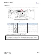
The ADM-PCIE-KU3 has a quad DIP switch SW1, located on the rear side of the board in the middle of the card
along the top edge. The function of each switch in SW1 is detailed below:
Figure 4 : Switches
Switch
Factory
Default
Function
OFF State
ON State
SW1-1
OFF
User
Switch
Pin AH12 = '1'
Pin AH12 = '0'
SW1-2
OFF
Flash
Lockdown
Flash block Lockdown enabled
Flash block Lockdown disabled
SW1-3
OFF
Xilinx/AD
Mode
Configure from Alpha Data region
Configure from Xilinx region
SW1-4
ON
Failsafe/
Default
Configure from failsafe region
Configure from default region
Table 3 : SW1 Switch Functions
Use IO Standard "LVCMOS33" when constraining the user switch pin.
Note:
SW1-1 is also used as a JTAG factory configuration switch when the TI Fusion programing box adapter is
plugged into the card. For normal operation of SW1-1 do not use it with the TI Fusion adapter card. If the TI
Fusion adapter card is present set SW1-1 ON to communicate with TI tools.
Page 5
Functional Description
ad-ug-1284_v1_13.pdf


