ADM-PA101 User Manual
3.3 PCI Express
The ADM-PA100 is capable of PCIe Gen 1/2/3 with 1/4/8/16 lanes and Gen 4 with 1/4/8 lanes. The ACAP drives
these lanes directly using the Integrated PCI Express block from Xilinx. Negotiation of PCIe link speed and
number of lanes is generally automatic and does not require user intervention.
PCI Express reset (PERST#) is connected to the ACAP through a buffer. See
signal
PERST_PL_L for fabric accessible location, and PCIE_RST_1V8_L for the PS location.
The pin assignments for the high speed lanes are provided in the pinout attached to the
,
see net names PCIE_TX*_PIN_P/N and PCIE_RX*_P/N.
3.4 DDR4 SDRAM
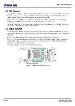
Two banks of DDR4 SDRAM memory are soldered down to the board. The available density of the memory is
4GB/per bank, 8GB total. The memory interface is 72-bit wide data (64 data + 8 ECC). Maximum signaling rate is
3200 MT/s.
Memory solutions are available from the Xilinx (See Xilinx PG313 Versal ACAP Programmable
Network on Chip and Integrated Memory Controller v1.0). DDR4_0 uses the Non-Flipped Pinout, and DDR4_1
uses the Flipped Pinout. An example memory exerciser project is included in the RD-PA101. All pin location
The 4Gb components used are Micron MT40A1G16RC-062E
Figure 7 : DDR4 bank locations by index
Page 12
Functional Description
ad-ug-1430_v1_2.pdf


