background image

ADM-PA101 User Manual


3.2.1 Si5328

If jitter attenuation is required please see the reference documentation for the Si5328.

www.silabs.com/Support%20Documents/TechnicalDocs/Si5328.pdf

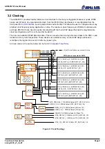
There are two input clock options. Si5328 pin CLKIN1 (board net name SI5328_REFCLK_IN_P/N) of the Si5328

is connected to an MGT clock output for the most direct clock recovery architecture. Si5328 pin CLKIN2 (board

net name MGT_PROGCLK_6_P/N) of the Si5328 is connected to a programable clock from the onboard clock

synthesizer.

The two output clocks are connected to quads 201 and 204 to provide clocking capability to the entire FMC+

interface.

The INT_C1B and LOL signals for the Si5328 is available for use, and can be located at net names

SI5328_1V5_INT_C1B and SI5328_1V5_LOL in the 

Complete Pinout Table

.

The active low reset of the Si5328 is accessible to the ACAP. See net names SI5328_1V5_RST_L in the

Complete Pinout Table

.

Note: 

Each sideband signal has an external pull-up resistor.

The Si5328 configuration register map is volatile, and must be written on each power up event over I2C. Use

nets SI5328_1V5_SDA and SI5328_1V5_SCL at pins located in the 

Complete Pinout Table

. The Si5328 device

is configured the I2C address shown in the table below:

device

7bit Hex Address

Binary Address

Si5328

68

110_1000

Table 5 : Si5328 address table

3.2.2 PCIe Reference Clocks

The 16 MGT lanes connected to the PCIe card edge use MGT tiles 103 through 106 and use the host system's

100 MHz PCIe reference clock (net name PCIE_REFCLK_0_P/N or PCIE_REFCLK_1_P/N in the 

Complete

Pinout Table

).

Alternatively, a more stable but asynchronous onboard 100MHz clock is available as well (net name

PCIE_LCL_REFCLK_P/N in the 

Complete Pinout Table

).

3.2.3 Fabric Clock

The design offers a fabric clock (net name FABRIC_CLK_P/N) which defaults to 300 MHz. This clock is intended

to be used for IDELAY elements in PL designs. The fabric clock is connected to a Global Clock (GC) pin. This

clock frequency can be changed to any arbitrary clock frequency up to 350MHz by re-programing the Si5338

reprogrammable clock oscillator. See details on avr2util in the section: 

Micro USB Interface

.

Use constraints DIFF_TERM_ADV = TERM_100 and IOSTANDARD LVDS15 for this reference clock.

See net names FABRIC_CLK_P/N in the 

Complete Pinout Table

 for pin locations.

3.2.4 PS Reference Clock (PS_REF_CLK)

A 50MHz clock is fed into the dedicated REF_CLK_503 pin to drive the processor system.

3.2.5 MGT Programable Clock

The MGT reference clock connects to each quad connected to the FMC connector, the Si5328, and the FireFly

Page 10

Functional Description

ad-ug-1430_v1_2.pdf

Содержание ADM-PA100

Страница 1: ...ADM PA101 User Manual Document Revision 1 2 December 13th 2021...

Страница 2: ...prior written consent from Alpha Data Parallel Systems Ltd Head Office Address Suite L4A 160 Dundee Street Edinburgh EH11 1DQ UK Telephone 44 131 558 2600 Fax 44 131 558 2700 email sales alpha data co...

Страница 3: ...gramable Clock 10 3 2 6 FMC Clocks 11 3 2 7 Samtec FireFly Clock 11 3 2 8 Memory Clocks 11 3 3 PCI Express 12 3 4 DDR4 SDRAM 12 3 5 FMC Interface 13 3 6 FireFly 15 3 7 System Monitor 16 3 7 1 System M...

Страница 4: ...Table 9 Boot Mode Selection 21 Table 10 MIO Map 25 Table 11 Complete Pinout Table 28 List of Figures Figure 1 ADM PA101 Product Photo 1 Figure 2 Thermal Performance 5 Figure 3 ADM PA101 Block Diagram...

Страница 5: ...VSVA2197 package FMC front panel interface 24 high speed serial channels capable of 32Gbps each 160 single ended general purpose signals 80 differential pairs 1 5 1 0V VADJ voltage range Extra clearan...

Страница 6: ...ADM PA101 User Manual 1 2 Order Code See the PA101 datasheet for complete ordering options Page 2 Introduction ad ug 1430_v1_2 pdf...

Страница 7: ...PCI Express CEM revision 4 0 Description Measure Total Dy 126 3 mm PCB Dy 111 15 mm Total Dx 267 2 mm PCB Dx 254 mm Total Dz 19 6 mm Circuit assembly weight 210 grams Total weight with heat sink 730...

Страница 8: ...Ie Edge though it does use 3 3V AUX To operate with PCIe edge only ensure SW1 8 is OFF see Switches As per PCIe specification users should limit the board power consumption to 66W when using only the...

Страница 9: ...emperature to your system ambient and select user override for the effective theta JA Then enter the figure associated with your system LFM in the blank field Proceed to enter all applicable design el...

Страница 10: ...form with the Versal XCVC1902 a full FMC interface PCIe Gen3x16 or 2xGen4x8 interface two banks of DDR4 3200 each 72 bits wide for 64 bits with 8 bits ECC GEM0 Ethernet QSPI uSD USB UART a Digilent PM...

Страница 11: ...l power up Immediately power down SW2 1 OFF Factory Configuration Normal operation SW2 2 ON Factory Configuration Normal operation SW2 3 OFF HOST_I2C_EN System Monitor connected to PCIe slot I2C Syste...

Страница 12: ...igure 5 Front Panel LEDs Comp Ref Function Net Name ON State OFF State D6 USER_LED_G1_1V8 User defined 0 User defined 1 D11 USER_LED_G0_1V8 User defined 0 User defined 1 D12 ERROR_OUT_L Boot error No...

Страница 13: ...1101000 CMODE GND I2C CNTRL CLKOUT2 CLKOUT1 Crystal 114 285MHz XA XB CLKIN1 CLKIN2 FPGA Bank 710 SI5328_1V5_SDA SI5328_1V5_SCL SI5328_0_RST_1V5_L SI5328_1V5_INT_C1B SI5328_1V5_C2B SI5328_1V5_LOL MGT_P...

Страница 14: ...ddress shown in the table below device 7bit Hex Address Binary Address Si5328 68 110_1000 Table 5 Si5328 address table 3 2 2 PCIe Reference Clocks The 16 MGT lanes connected to the PCIe card edge use...

Страница 15: ...cted to the FMC site are also configured such that they can be clocked from the Si5328 jitter attenuator or the onboard Si5338 clock synthesizer Pin locations of net names SI5328_ _OUT_P N and MGT_PRO...

Страница 16: ...to the Complete Pinout Table see net names PCIE_TX _PIN_P N and PCIE_RX _P N 3 4 DDR4 SDRAM Two banks of DDR4 SDRAM memory are soldered down to the board The available density of the memory is 4GB per...

Страница 17: ...ystem monitor AVR2UTIL application Alpha Data provides a wide range of compatible FMC cards Please see www alpha data com products io adaptors or contact sales alpha data com for more details It is po...

Страница 18: ...66 67 HA 16 2 15 diff Pairs 30 single ended HA_CC 1 0 2x Regional Clocks GPIO pairs 4 single ended HA 23 18 6 diff Pairs 12 single ended HA_CC 17 Regional Clock GPIO pair 2 single ended HB_0 64 HB 5...

Страница 19: ...orted by the Xilinx GTY Transceivers Please see Xilinx User Guide UG578 for more details on the capabilities of the transceivers All FireFly sites have control signals connected to the ACAP Their conn...

Страница 20: ...rom PCIe Edge in amps 3V3_AUX ADC03 3 3V auxiliary board input supply from PCIE edge 3V3_DIG ADC04 3 3V generated onboard for FMC and other circuits 3V3_VCCO ADC05 3 3V generated onboard for ACAP IO v...

Страница 21: ...y Powered off Flashing Green Flashing Red together Attention critical alarm active Flashing Green Flashing Red alternating Service Mode Flashing Green Red Attention alarm active Red Missing applicatio...

Страница 22: ...s interface Avr2util for Windows and the associated USB driver is downloadable here https support alpha data com pub firmware utilities windows Avr2util for Linux is downloadable here https support al...

Страница 23: ...do projects xpr format that are available for customers in the early access section of the PA101 You can request access to them by messaging support alpha data com Every early access project contain t...

Страница 24: ...sign_name bif w o BOOT BIN Note You may first need to run settings32 bat settings64 bat in your current Vivado installation path depending if yours is a 32 or 64 bits OS Prepare the uSD card by format...

Страница 25: ...m monitor can drive the MODE pins low open drain drive so it is recommended to leave the switches in the OFF positions or set to SD 3 0 boot mode From there the user can issue commands to change the b...

Страница 26: ...hub which can be accessed at either the front or the back edge of the card UART0 passes through an FT2232HQ USB to UART converter This is the same IC that performs the USB to JTAG conversion This UAR...

Страница 27: ...User EEPROM A 2Kb I2C user EEPROM is provided for storing MAC addresses or other user information The EEPROM is part number CAT34C02HU4IGT4A The address pins A2 A1 and A0 are all strapped to a logica...

Страница 28: ...ADM PA101 User Manual Page Intentionally left blank Page 24 Functional Description ad ug 1430_v1_2 pdf...

Страница 29: ...lel Quad SPI M31 PMC_MIO13_500 USB_ULPI_RST USB 2 0 K31 PMC_MIO14_500 USB_ULPI_DATA 0 USB 2 0 J31 PMC_MIO15_500 USB_ULPI_DATA 1 USB 2 0 H31 PMC_MIO16_500 USB_ULPI_DATA 2 USB 2 0 G31 PMC_MIO17_500 USB_...

Страница 30: ...MIO50_501 PMC_I2C_SCL Not Used G17 PMC_MIO51_501 PMC_I2C_SDA Not Used A39 LPD_MIO0_502 GEM0_TX_CLK GEM0 Ethernet B39 LPD_MIO1_502 GEM0_TX_DATA 0 GEM0 Ethernet C39 LPD_MIO2_502 GEM0_TX_DATA 1 GEM0 Ethe...

Страница 31: ...IO GPIO J4 at rear D34 LPD_MIO20_502 GPIO GPIO J4 at rear C34 LPD_MIO21_502 GPIO GPIO J4 at rear B34 LPD_MIO22_502 GPIO GPIO J4 at rear A34 LPD_MIO23_502 GPIO GPIO J4 at rear C33 LPD_MIO24_502 GEM0_MD...

Страница 32: ...2 DDR4_0_A11 IO_L25P_N8P2_M0P50_700 1 2 AF46 DDR4_0_A12 IO_L0N_XCC_N0P1_M0P1_700 1 2 AF43 DDR4_0_A13 IO_L24N_GC_XCC_N8P1_M0P49_700 1 2 AJ40 DDR4_0_A14 IO_L16N_N5P3_M0P33_700 1 2 AH41 DDR4_0_A15 IO_L14...

Страница 33: ...2 AM40 DDR4_0_DQ10 IO_L16N_N5P3_M0P87_701 1 2 AM38 DDR4_0_DQ11 IO_L17N_N5P5_M0P89_701 1 2 AM41 DDR4_0_DQ12 IO_L14N_N4P5_M0P83_701 1 2 AK37 DDR4_0_DQ13 IO_L13P_N4P2_M0P80_701 1 2 AM39 DDR4_0_DQ14 IO_L...

Страница 34: ...4_701 1 2 AR45 DDR4_0_DQ43 IO_L11N_N3P5_M0P77_701 1 2 AU44 DDR4_0_DQ44 IO_L8N_N2P5_M0P71_701 1 2 AP43 DDR4_0_DQ45 IO_L7P_N2P2_M0P68_701 1 2 AT44 DDR4_0_DQ46 IO_L8P_N2P4_M0P70_701 1 2 AR44 DDR4_0_DQ47...

Страница 35: ..._M0P96_701 1 2 AK39 DDR4_0_DQS1_C IO_L15N_XCC_N5P1_M0P85_701 1 2 AL39 DDR4_0_DQS1_T IO_L15P_XCC_N5P0_M0P84_701 1 2 AG46 DDR4_0_DQS2_C IO_L3N_XCC_N1P1_M0P7_700 1 2 AH46 DDR4_0_DQS2_T IO_L3P_XCC_N1P0_M0...

Страница 36: ...28 DDR4_1_A8 IO_L25N_N8P3_M1P159_705 1 2 BF26 DDR4_1_A9 IO_L4P_N1P2_M1P116_705 1 2 BF28 DDR4_1_ACT_N IO_L3N_XCC_N1P1_M1P115_705 1 2 BA32 DDR4_1_ALERT_N IO_L25N_N8P3_M1P105_704 1 2 BG29 DDR4_1_BA0 IO_L...

Страница 37: ...P_N4P2_M1P80_704 1 2 AV34 DDR4_1_DQ21 IO_L14N_N4P5_M1P83_704 1 2 AP33 DDR4_1_DQ22 IO_L17P_N5P4_M1P88_704 1 2 AW33 DDR4_1_DQ23 IO_L16N_N5P3_M1P87_704 1 2 AV31 DDR4_1_DQ24 IO_L20P_N6P4_M1P94_704 1 2 AM3...

Страница 38: ...1_703 1 2 BB38 DDR4_1_DQ53 IO_L11P_N3P4_M1P22_703 1 2 BC36 DDR4_1_DQ54 IO_L8N_N2P5_M1P17_703 1 2 BC40 DDR4_1_DQ55 IO_L7P_N2P2_M1P14_703 1 2 AV35 DDR4_1_DQ56 IO_L16N_N5P3_M1P33_703 1 2 AU36 DDR4_1_DQ57...

Страница 39: ..._1_DQS5_C IO_L0N_XCC_N0P1_M1P55_704 1 2 BF33 DDR4_1_DQS5_T IO_L0P_XCC_N0P0_M1P54_704 1 2 BD38 DDR4_1_DQS6_C IO_L6N_GC_XCC_N2P1_M1P13_703 1 2 BD39 DDR4_1_DQS6_T IO_L6P_GC_XCC_N2P0_M1P12_703 1 2 AW37 DD...

Страница 40: ...T M6 DP14_C2M_N GTY_TXN2_203 MGT M7 DP14_C2M_P GTY_TXP2_203 MGT M1 DP14_M2C_N GTY_RXN2_203 MGT M2 DP14_M2C_P GTY_RXP2_203 MGT L8 DP15_C2M_N GTY_TXN3_203 MGT L9 DP15_C2M_P GTY_TXP3_203 MGT L3 DP15_M2C_...

Страница 41: ...MGT F2 DP21_M2C_P GTY_RXP1_205 MGT E8 DP22_C2M_N GTY_TXN2_205 MGT E9 DP22_C2M_P GTY_TXP2_205 MGT F5 DP22_M2C_N GTY_RXN2_205 MGT F6 DP22_M2C_P GTY_RXP2_205 MGT D10 DP23_C2M_N GTY_TXN3_205 MGT D11 DP23_...

Страница 42: ...N_VCC_INT_MIO PMC_MIO40_501 1 8 A32 ERROR_OUT ERROR_OUT_503 1 5 AR1 FABRIC_CLK_N IO_L9N_GC_XCC_N3P1_M3P73_710 1 5 AR2 FABRIC_CLK_P IO_L9P_GC_XCC_N3P0_M3P72_710 1 5 L37 FAN_FAIL_1V8_L IO_L0N_306 1 8 C1...

Страница 43: ...CLK3_PIN_P GTY_REFCLKP1_203 MGT REFCLK D14 GBTCLK5_PIN_N GTY_REFCLKN1_205 MGT REFCLK D15 GBTCLK5_PIN_P GTY_REFCLKP1_205 MGT REFCLK C33 GEM0_MDC LPD_MIO24_502 3 3 D33 GEM0_MDIO LPD_MIO25_502 3 3 C19 GE...

Страница 44: ..._M2P146_708 FMC_VADJ AP13 HA09_N IO_L23N_N7P5_M2P155_708 FMC_VADJ AN14 HA09_P IO_L23P_N7P4_M2P154_708 FMC_VADJ AV14 HA10_N IO_L17N_N5P5_M2P143_708 FMC_VADJ AV15 HA10_P IO_L17P_N5P4_M2P142_708 FMC_VADJ...

Страница 45: ...M3P5_709 FMC_VADJ BA3 HB02_P IO_L2P_N0P4_M3P4_709 FMC_VADJ AY4 HB03_N IO_L10N_N3P3_M3P21_709 FMC_VADJ AY5 HB03_P IO_L10P_N3P2_M3P20_709 FMC_VADJ BB1 HB04_N IO_L3N_XCC_N1P1_M3P7_709 FMC_VADJ BA1 HB04_P...

Страница 46: ...B20_N IO_L13N_N4P3_M3P27_709 FMC_VADJ BF8 HB20_P IO_L13P_N4P2_M3P26_709 FMC_VADJ BE7 HB21_N IO_L17N_N5P5_M3P35_709 FMC_VADJ BD8 HB21_P IO_L17P_N5P4_M3P34_709 FMC_VADJ AY18 LA00_CC_N IO_L24N_GC_XCC_N8P...

Страница 47: ...BB20 LA15_P IO_L1P_N0P2_M2P56_707 FMC_VADJ AY19 LA16_N IO_L25N_N8P3_M2P105_707 FMC_VADJ AW20 LA16_P IO_L25P_N8P2_M2P104_707 FMC_VADJ BC16 LA17_CC_N IO_L6N_GC_XCC_N2P1_M2P67_707 FMC_VADJ BB16 LA17_CC_P...

Страница 48: ..._L1N_N0P3_M2P3_706 FMC_VADJ BG25 LA32_P IO_L1P_N0P2_M2P2_706 FMC_VADJ BG23 LA33_N IO_L5N_N1P5_M2P11_706 FMC_VADJ BF24 LA33_P IO_L5P_N1P4_M2P10_706 FMC_VADJ C36 LDP_MIO12 LPD_MIO12_502 3 3 B36 LDP_MIO1...

Страница 49: ...IN_N GTY_REFCLKN1_206 MGT REFCLK B15 MGT_PROGCLK_7_PIN_P GTY_REFCLKP1_206 MGT REFCLK R40 PCIE_LCL_REFCLK_PIN_N GTY_REFCLKN0_104 MGT REFCLK R39 PCIE_LCL_REFCLK_PIN_P GTY_REFCLKP0_104 MGT REFCLK W40 PCI...

Страница 50: ...PCIE_RX8_P GTY_RXP3_104 MGT P47 PCIE_RX9_N GTY_RXN2_104 MGT P46 PCIE_RX9_P GTY_RXP2_104 MGT A44 PCIE_TX0_PIN_N GTY_TXN3_106 MGT A43 PCIE_TX0_PIN_P GTY_TXP3_106 MGT B42 PCIE_TX1_PIN_N GTY_TXN2_106 MGT...

Страница 51: ...MGT P42 PCIE_TX9_PIN_N GTY_TXN2_104 MGT P41 PCIE_TX9_PIN_P GTY_TXP2_104 MGT M37 PERST_PL_L IO_L0P_306 1 8 J34 PL_SCL IO_L9P_306 1 8 J35 PL_SDA IO_L9N_306 1 8 F17 PMC_I2C_SCL PMC_MIO50_501 1 8 G17 PMC...

Страница 52: ..._M3P57_710 1 5 AU3 SI5328_1V5_LOL IO_L3N_XCC_N1P1_M3P61_710 1 5 AV3 SI5328_1V5_RATE0 IO_L2N_N0P5_M3P59_710 1 5 AT3 SI5328_1V5_RATE1 IO_L3P_XCC_N1P0_M3P60_710 1 5 AT1 SI5328_1V5_SCL IO_L0N_XCC_N0P1_M3P...

Страница 53: ...ULPI_DATA 4 PMC_MIO19_500 1 8 J30 USB_ULPI_DATA 5 PMC_MIO20_500 1 8 K30 USB_ULPI_DATA 6 PMC_MIO21_500 1 8 L30 USB_ULPI_DATA 7 PMC_MIO22_500 1 8 M30 USB_ULPI_DIR PMC_MIO23_500 1 8 L29 USB_ULPI_NXT PMC_...

Страница 54: ...updates 14 January 2022 1 2 K Roth Added example of changing boot modes to section Boot Modes Address Suite L4A 160 Dundee Street Edinburgh EH11 1DQ UK Telephone 44 131 558 2600 Fax 44 131 558 2700 em...

Отзывы: