


3–3
Module Programming
Publication 17946.5.2 - May 1996
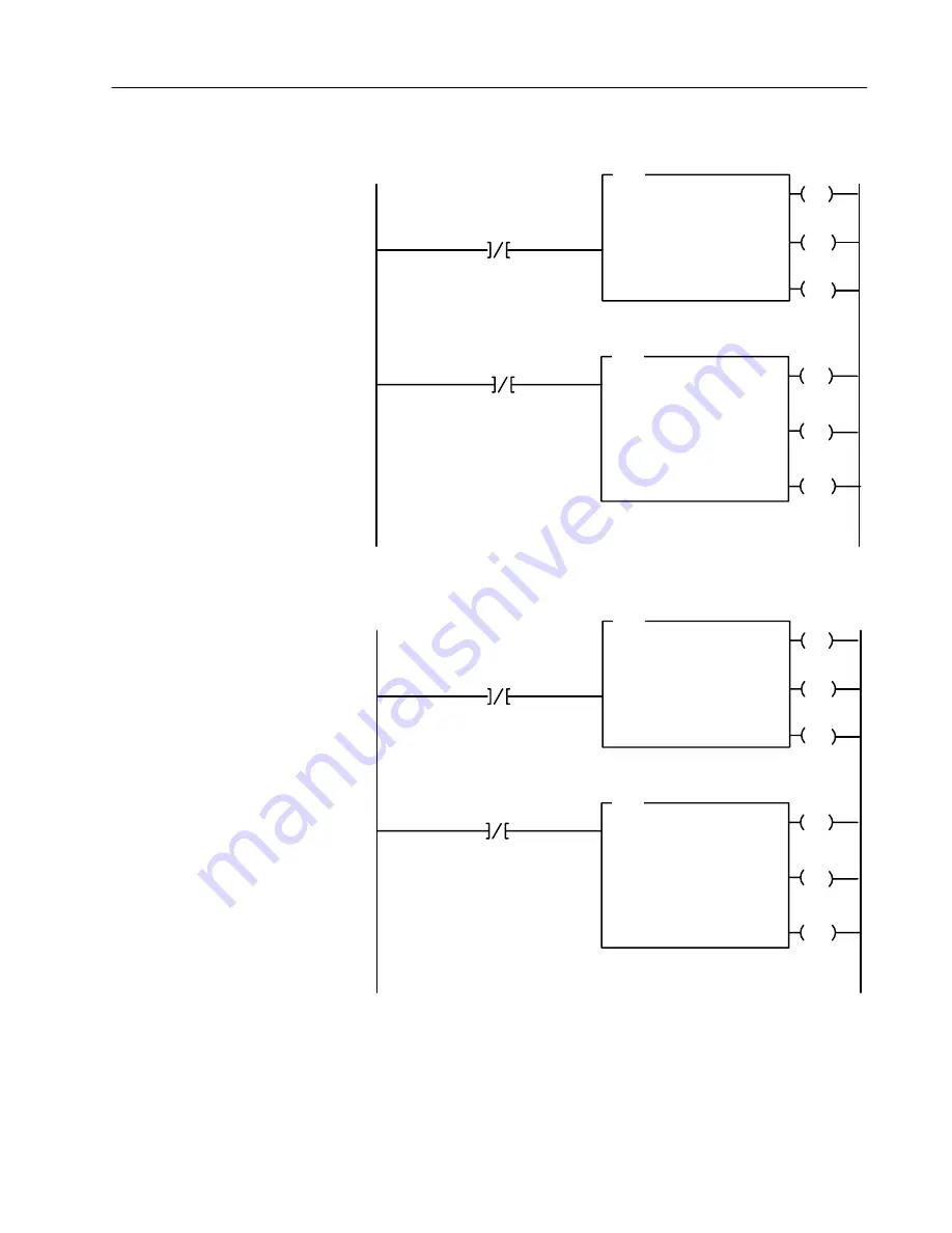
Figure 3.2
PLC3 Family Sample Program Structure for a 1794OE4 Module
EN
BTR
BLOCK XFER READ
RACK:
GROUP:
MODULE:
CONTROL:
7
1
0
#B6:0
DATA FILE:
LENGTH:
#B7:0
1
EN
BTW
BLOCK XFER WRITE
RACK:
GROUP:
MODULE:
CONTROL:
7
1
0
#B6:0
DN
DATA FILE:
LENGTH:
#B8:0
14
B6:0
05
Block Transfer
Read Done Bit
ER
Enable
Done
Error
12
15
13
Enable
Done
Error
02
05
03
Block Transfer
Write Done Bit
1
DN
ER
B6:0
15
Program Action
At powerup in RUN mode, or when the
processor is switched from PROG to RUN,
the user program enables a block transfer
read. Then it initiates a block transfer write
to configure the module and send data
values.
Thereafter, the program continuously
performs read block transfers and write
block transfers.
Note: You must create the data file
for the block transfers before you
enter the block transfer instructions.
2
Figure 3.3
PLC3 Family Sample Program Structure for a 1794IE4XOE2 Module
EN
BTR
BLOCK XFER READ
RACK:
GROUP:
MODULE:
CONTROL:
7
2
0
#B9:0
DATA FILE:
LENGTH:
#B10:0
5
EN
BTW
BLOCK XFER WRITE
RACK:
GROUP:
MODULE:
CONTROL:
7
2
0
#B9:0
DN
DATA FILE:
LENGTH:
#B11:0
8
B9:0
05
Block Transfer
Read Done Bit
ER
Enable
Done
Error
12
15
13
Enable
Done
Error
02
05
03
Block Transfer
Write Done Bit
1
2
DN
ER
B9:0
15
Program Action
At powerup in RUN mode, or when the
processor is switched from PROG to RUN,
the user program enables a block transfer
read. Then it initiates a block transfer write
to configure the module and send data val
ues
Thereafter, the program continuously
performs read block transfers and write
block transfers.
Note: You must create the data file
for the block transfers before you
enter the block transfer instructions.