


[AKD4753-A]
AKD4753-A
AK4753 Evaluation Board Rev.2
GENERAL DESCRIPTION
The AKD4753-A is an evaluation board for AK4753, 2-in, 4-out CODEC with DSP Functions. The
AKD4753-A has the Digital Audio I/F and can achieve the interface with digital audio systems via
optical connector.
■
Ordering guide
AKD4753-A --- Evaluation Board for AK4753
(Control software and USB cable are packed with this.)
FUNCTION
•
RCA connectors for analog audio input/output
•
Optical connector for digital audio input
•
On-board digital audio interface (AK4118A)
•
Potentiometers for Volume and Bass gain control
•
USB connector for serial control interface
•
1k bits EEPROM
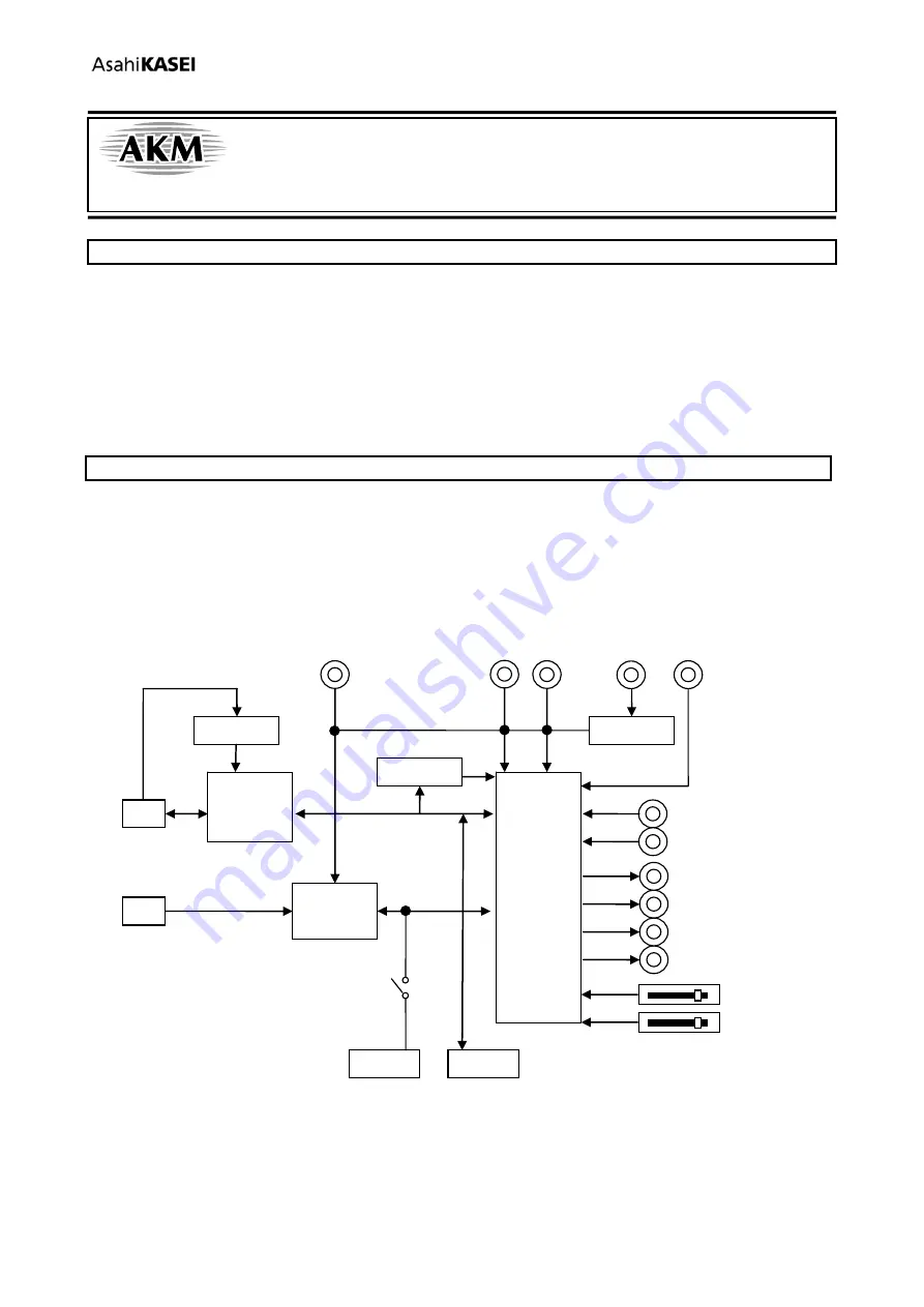
AK4753
AINL
DSP
LOUT1
ROUT2
ROUT1
LOUT1
AINR
3.3V
10 Pin Header
EEPROM
PIC4550
I2C
10 Pin Header
Regulator
USB 3.3V
Regulator
PORT1
Opt In
PORT4
USB
PORT3 PORT2
AK4118A
(DIR)
SAIN2
SAIN1
Volume
Bass Gain
Potentiometer
GND
+5V
AVDD
DVDD
D3.3V
Figure 1. AKD4753-A Block Diagram
* Circuit diagram and PCB layout are attached at the end of this manual.
KM103902
2011/01
- 1 -


