AKM AKD4637-B Скачать руководство пользователя страница 19


[AKD4637-B] 

<KM120603> 


2018/10 


- 19 - 


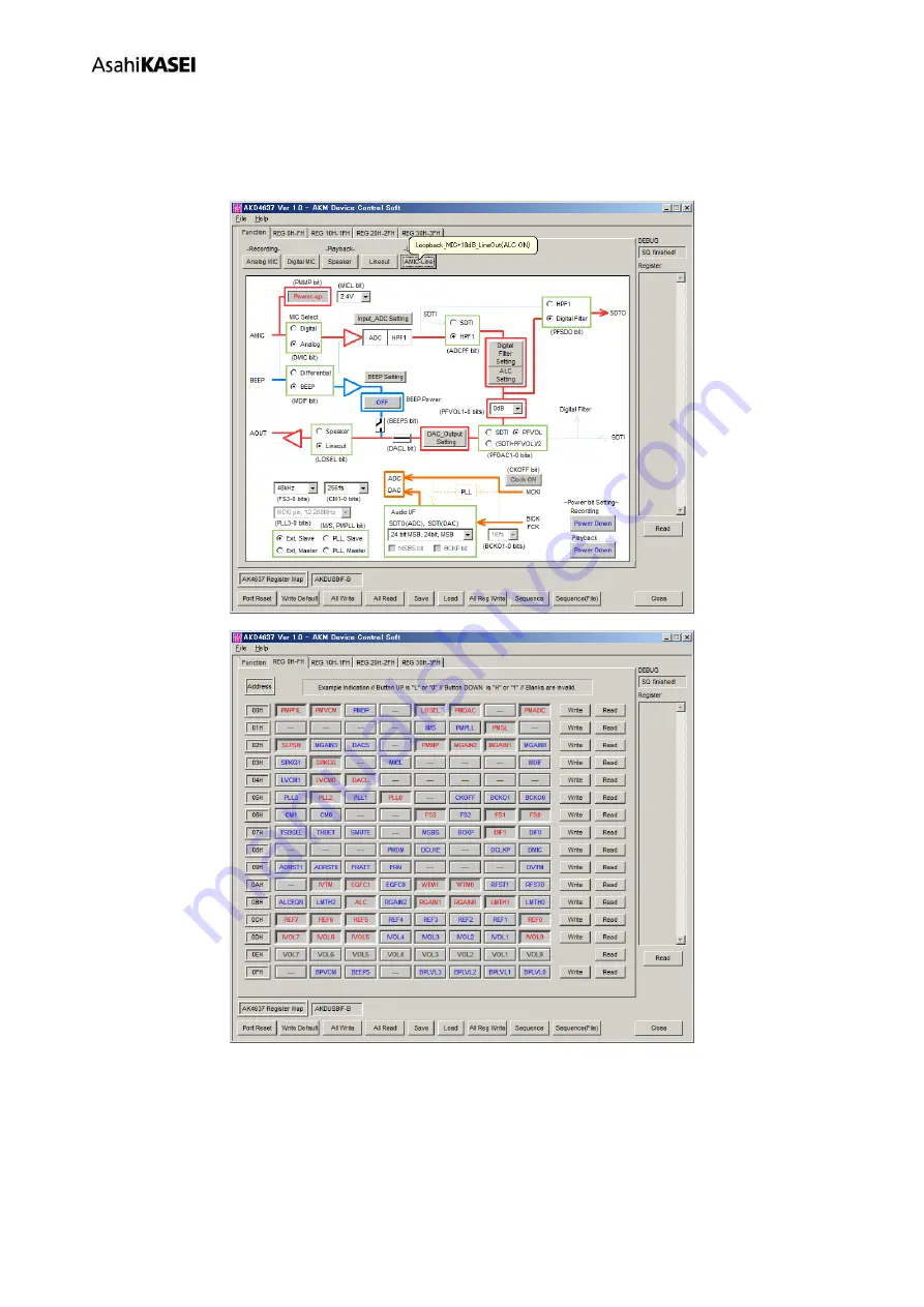
(1-1-5)  [AMIC-Line (Loopb18dB_LineOut(ALC ON))] Sequential process 


When [AMIC-Line] button in the main window is clicked, the sequence of Loopback settings is executed. (

Note 2

) 


Figure 14. [AMIC-Line] Setting (After) 


Содержание AKD4637-B

Страница 1: ...ion board for AK4637 Control software is included in this package FUNCTION Compatible with 2 types of interface Direct interface with AKM s A D converter evaluation boards DIT DIR with optical input o...

Страница 2: ...2 In case of supplying the power from regulator JP13 AVDDSEL JP11 USB5V 5V 3 3V Name of Jack Color Default Setting Using REG1 red 5V for regulator input GND1 black 0V ground Table 1 Set up of power s...

Страница 3: ...upports 256fs and 512fs When evaluating in a condition except above please use other mode Refer to the datasheet for register setting of the AK4637 Applicable Evaluation Mode 1 A D Evaluation using th...

Страница 4: ...he AK4118A and SDTO of the AK4637 is output to the AK4118A The jumper pins should be set as follows JP5 MCKI JP6 BICK JP7 FCK DIR EXT DIR EXT JP8 DIR EXT SDTO 2 Evaluation of D A using DIR of AK4118A...

Страница 5: ...TI BCLK FCK SDTI SDTO MCKI 1fs 16fs 32fs 64fs 11 2896MHz 12MHz 12 288MHz 13 5MHz 24MHz 27MHz Figure 2 PLL Master Mode 3 2 Setting in PLL Slave Mode A reference clock of PLL is selected among the input...

Страница 6: ...egisters of the AK4637 should be set to EXT Slave Mode MCLK BICK FCK and SDTI are input into JP5 JP6 JP7 and JP9 SDTO is output from JP8 AK4951EN DSP or P MCKI BICK LRCK SDTO SDTI BCLK LRCK SDTI SDTO...

Страница 7: ...PORT1 DIR and PORT2 DIT Registers of the AK4637 should be set to PLL Slave Mode Reference Clock BICK BICK and FCK should be supplied to JP6 and JP7 The jumper pins should be set as follows JP5 MCKI J...

Страница 8: ...t Right justified H L O 64fs O 3 0 1 1 24bit Left justified 24bit Right justified H L O 64fs O 4 1 0 0 24bit Left justified 24bit Left justified H L O 64fs O Default 5 1 0 1 24bit I2 S 24bit I2 S L H...

Страница 9: ...JP2 should be set to open JP3 IN JP1 S D JP2 IN AIN MPWR 1 2 IN IN Input Circuit Differential input IN and IN are input to J1 When the Mic Power is not used JP2 and JP3 should be set to open JP3 IN J...

Страница 10: ...OUT SPP SPN Output Circuit 2 1 SPP SPN Output Circuit Default SPP and SPN are output from TP3 and TP4 JP4 AOUT 2 2 Monaural Line Output Circuit AOUT is output from J2 JP4 AOUT AKM assumes no responsib...

Страница 11: ...The USB control is recognized as HID Human Interface Device on the PC 4 Double click the icon akd4637 exe to open the control program Note 1 When the screen does not display AKDUSBIF B at bottom left...

Страница 12: ...s button to initialize the registers 3 All Write Executes write commands for all registers displayed 4 All Read Executes read commands for all registers displayed 5 Save Save Address of Register dialo...

Страница 13: ...on each button Refer to 1 1 1 Path and Each Setting block Executes a setup of the path or functions Refer to 1 1 2 Explanation of the color of a pass line Thick lines blue red yellow and sour orange s...

Страница 14: ...Digi Fil SDTO Digital MIC Recording_DigitalMIC ALC ON Digital MIC Input Recording DMDAT DMCLK SDTO DMDAT DMCLK Deci Fil Digi Fil SDTO Speaker Playback_Speaker 8 4dB ALC ON Speaker Output SDTI SPP SPN...

Страница 15: ...dB ALC ON Sequential process When Analog MIC button in the main window is clicked the sequence for MIC input Settings is executed Note 2 Figure 10 Analog MIC Setting After Note 2 The function button m...

Страница 16: ...10 16 1 1 2 Digital MIC Recording_DigitalMIC ALC ON Sequential process When Digital MIC button in the main window is clicked the sequence for Digital MIC input Settings is executed Note 2 Figure 11 D...

Страница 17: ...3 2018 10 17 1 1 3 Speaker Playback_Speaker 8 4dB ALC ON Sequential process When Speaker button in the main window is clicked the sequence for Speaker output Settings is executed Note 2 Figure 12 Spea...

Страница 18: ...KM120603 2018 10 18 1 1 4 Lineout Playback_Lineout Sequential process When Lineout button in the main window is clicked the sequence for Line output Settings is executed Note 2 Figure 13 Line out Set...

Страница 19: ...2018 10 19 1 1 5 AMIC Line Loopback_MIC 18dB_LineOut ALC ON Sequential process When AMIC Line button in the main window is clicked the sequence of Loopback settings is executed Note 2 Figure 14 AMIC...

Страница 20: ...BEEP Setting button Opens BEEP Setting dialog box BEEP Power OFF ON button The path of a BEEP output is controlled and performs a BEEPS output OFF ON ON BEEPS is set 1 and BEEPS bit Switch is connect...

Страница 21: ...er Down PMADC PMDM 0 PMPFIL 0 Note 7 Playback Power Down Up Button Register bit Setup value Power Up PMVCM 1 Note 5 DACS or DACL When LOSEL bit 0 DACS bit 1 When LOSEL bit 1 DACL bit 1 PMPFIL When PFD...

Страница 22: ...ouse operation Button Down indicates 1 and the bit name is shown in red when read only the name is shown in dark red Button Up indicates 0 and the bit name is shown in blue when read only the name is...

Страница 23: ...is not checked the data will become 0 Click OK to write the set values to the registers or click Cancel to cancel this setting Figure 17 Register Set Window 2 2 Read Data Read Click the Read button l...

Страница 24: ...heck box When the All Address checkbox is checked all register settings will be saved Start Address edit box When the All Address check box is not checked set starts register address to save End Addre...

Страница 25: ...le assignment mar Close button Closes the dialog box and finish the process All Write flame Executes all register write Selected files are executed in descending order Start button Start the register...

Страница 26: ...this dialog box Figure 20 Sequence Window Sequence Setting Set register sequence according to the following process 1 Select a command Use Select pull down box to choose commands Corresponding boxes w...

Страница 27: ...are shown below No use None Register Address Data Interval Reg_Mask Address Data Mask Interval Interval Interval Stop None End None Control Buttons Functions of Control Button are shown below DEL butt...

Страница 28: ...lected files are executed in descending order Stop button Stops the sequence process Help button Opens a help window Save button Saves a sequence setting file assignment The file name is mas Open righ...

Страница 29: ...o the datasheet for register definitions Figure 23 Audio I F Window Gain Control by Slider The volume can also be changed by slider When a value is input in the edit box the slider is moved to the val...

Страница 30: ...Opens the frequency response plot dialog Filter Plot Register writes of a filter factor are also executed Write button Calculation of all the filters and coefficient writing are executed Example Setti...

Страница 31: ...48 236 8 fs 48 kHz HPF2 Cut Off Frequency High Pass Filter 2 cut off frequency 0 0001 fc fs 0 497 LPF Cut Off Frequency Low Pass Filter cut off frequency 0 05 fc fs 0 497 5 Band Equalizer EQ1 5 Center...

Страница 32: ...gure 27 Register Setting for Filter Window Followings are the cases when a register set value is updated 1 When Register Setting button was pushed 2 When F Response button was pushed 3 When Write butt...

Страница 33: ...raph again Log View check button Switch of Linear Log display Mouse Control of Left Button radio button The item fo Gain which can be adjusted with a mouse can be chosen at using EQx Note 12 fo Center...

Страница 34: ...erated with the mouse and it is possible to set the filter characteristic on this screen The center frequency and the gain setting are changed by moving the mouse while left clicking Note 12 The setti...

Страница 35: ...ve Figure 32 This automatic compensation is effective to EQ which set the gain as 1 Note 12 Note 13 Note 14 Note 13 There is a possibility that the automatic compensation is not correctly done when th...

Страница 36: ...etup is returned the state of before pushing a button Please use the button when it expected that a noise continues Figure 33 Equalizer Gain Setting Button ON EQCx bit OFF EQxG5 0 bits 0x3F 0 03dB EQx...

Страница 37: ...efer to the datasheet for register definitions Figure 36 ALC Setting Window Volume Read When the Start button on the bottom right of the dialog is clicked reading VOL register is executed periodically...

Страница 38: ...k the DAC Setting button in the main window to open DAC setting dialog Output mode DAC and output gain setting are available The settings on this dialog are interlocked with the settings on register m...

Страница 39: ...Setting Dialog Box Click the BEEP Setting button in the main window to open BEEP setting dialog The settings on this dialog are interlocked with the settings on register map Refer to the datasheet for...

Страница 40: ...S N A weighted 88 1 dB MGAIN 0dB S N D 1dBFS 84 3 dB DR 60dBFS A Weighted 94 9 dB S N A weighted 95 0 dB ADC IN IN ADC SDTO IVOL 0dB ALC OFF MGAIN 18dB S N D 1dBFS 80 0 dB DR 60dBFS A Weighted 85 7 d...

Страница 41: ...ut MGAIN 18dB AK4637 ADC FFT 1dBFS 20 20k 50 100 200 500 1k 2k 5k 10k Hz 140 0 120 100 80 60 40 20 d B F S Figure 40 FFT Input level 1dBFS AK4637 ADC FFT 60dBFS 20 20k 50 100 200 500 1k 2k 5k 10k Hz 1...

Страница 42: ...signal 20 20k 50 100 200 500 1k 2k 5k 10k Hz 140 0 120 100 80 60 40 20 d B F S Figure 42 FFT No signal AK4637 ADC THD N vs Input Level fin 1kHz 100 0 90 80 70 60 50 40 30 20 10 dBr 100 60 95 90 85 80...

Страница 43: ...requency 1dBF 100 60 95 90 85 80 75 70 65 d B F S 20 20k 50 100 200 500 1k 2k 5k 10k Hz Figure 44 THD N vs Input Frequency AK4637 ADC Linearity fin 1kHz 120 0 100 80 60 40 20 dBr 120 0 100 80 60 40 20...

Страница 44: ...AKD4637 B KM120603 2018 10 44 AK4637 ADC Frequency Response 1dBFS 2k 20k 4k 6k 8k 10k 12k 14k 16k 18k Hz 2 0 1 8 1 6 1 4 1 2 1 0 8 0 6 0 4 0 2 d B F S Figure 46 Frequency Response...

Страница 45: ...7 ADC FFT 1dBFS 20 20k 50 100 200 500 1k 2k 5k 10k Hz 140 0 120 100 80 60 40 20 d B F S Figure 47 FFT Input level 1dBFS AK4637 ADC FFT 60dBFS 20 20k 50 100 200 500 1k 2k 5k 10k Hz 140 0 120 100 80 60...

Страница 46: ...signal 20 20k 50 100 200 500 1k 2k 5k 10k Hz 140 0 120 100 80 60 40 20 d B F S Figure 49 FFT No signal AK4637 ADC THD N vs Input Level fin 1kHz 100 0 90 80 70 60 50 40 30 20 10 dBr 100 60 95 90 85 80...

Страница 47: ...equency 1dBFS 20 20k 50 100 200 500 1k 2k 5k 10k Hz 100 60 95 90 85 80 75 70 65 d B F S Figure 51 THD N vs Input Frequency AK4637 ADC Linearity fin 1kHz 120 0 100 80 60 40 20 dBr 120 0 100 80 60 40 20...

Страница 48: ...AKD4637 B KM120603 2018 10 48 AK4637 ADC Frequency Response 1dBFS 2k 20k 4k 6k 8k 10k 12k 14k 16k 18k Hz 2 0 1 8 1 6 1 4 1 2 1 0 8 0 6 0 4 0 2 d B F S Figure 53 Frequency Response...

Страница 49: ...t MGAIN 18dB AK4637 ADC FFT 1dBFS 140 0 120 100 80 60 40 20 d B F S 20 20k 50 100 200 500 1k 2k 5k 10k Hz Figure 54 FFT Input level 1dBFS AK4637 ADC FFT 60dBFS 140 0 120 100 80 60 40 20 d B F S 20 20k...

Страница 50: ...signal 140 0 120 100 80 60 40 20 d B F S 20 20k 50 100 200 500 1k 2k 5k 10k Hz Figure 56 FFT No signal AK4637 ADC THD N vs Input Level fin 1kHz 100 0 90 80 70 60 50 40 30 20 10 dBr 100 60 95 90 85 80...

Страница 51: ...20 20k 50 100 200 500 1k 2k 5k 10k Hz 100 60 95 90 85 80 75 70 65 d B F S Figure 58 THD N vs Input Frequency C8 and C9 Ceramic Capacitor AK4637 ADC Linearity fin 1kHz 120 0 100 80 60 40 20 dBr 120 0 1...

Страница 52: ...AKD4637 B KM120603 2018 10 52 AK4637 ADC Frequency Response 1dBFS 2k 20k 4k 6k 8k 10k 12k 14k 16k 18k Hz 2 0 1 8 1 6 1 4 1 2 1 0 8 0 6 0 4 0 2 d B F S Figure 60 Frequency Response...

Страница 53: ...7 ADC FFT 1dBFS 20 20k 50 100 200 500 1k 2k 5k 10k Hz 140 0 120 100 80 60 40 20 d B F S Figure 61 FFT Input level 1dBFS AK4637 ADC FFT 60dBFS 20 20k 50 100 200 500 1k 2k 5k 10k Hz 140 0 120 100 80 60...

Страница 54: ...signal 20 20k 50 100 200 500 1k 2k 5k 10k Hz 140 0 120 100 80 60 40 20 d B F S Figure 63 FFT No signal AK4637 ADC THD N vs Input Level fin 1kHz 100 0 90 80 70 60 50 40 30 20 10 dBr 100 60 95 90 85 80...

Страница 55: ...quency 1dBFS 20 20k 50 100 200 500 1k 2k 5k 10k Hz 100 60 95 90 85 80 75 70 65 d B F S Figure 65 THD N vs Input Frequency AK4637 ADC Linearity fin 1kHz 120 0 100 80 60 40 20 dBr 120 0 100 80 60 40 20...

Страница 56: ...AKD4637 B KM120603 2018 10 56 AK4637 ADC Frequency Response 1dBFS 2k 20k 4k 6k 8k 10k 12k 14k 16k 18k Hz 2 0 1 8 1 6 1 4 1 2 1 0 8 0 6 0 4 0 2 d B F S Figure 67 Frequency Response...

Страница 57: ...SPK FFT 0 5dBFS SPKG 01 20 20k 50 100 200 500 1k 2k 5k 10k Hz 140 0 120 100 80 60 40 20 d B r A Figure 68 FFT Input level 0 5dBFS AK4637 DAC SPK FFT 60dBFS SPKG 01 20 20k 50 100 200 500 1k 2k 5k 10k H...

Страница 58: ...SPKG 01 20 20k 50 100 200 500 1k 2k 5k 10k Hz 140 0 120 100 80 60 40 20 d B r A Figure 70 FFT No signal AK4637 DAC SPK Out of band noise SPKG 01 20 100k 50 100 200 500 1k 2k 5k 10k 20k 50k Hz 140 0 1...

Страница 59: ...0 5dBFS SPKG 01 20 20k 50 100 200 500 1k 2k 5k 10k Hz 120 40 110 100 90 80 70 60 50 d B Figure 72 THD N vs Input Frequency AK4637 DAC SPK Linearity fin 1kHz SPKG 01 100 0 90 80 70 60 50 40 30 20 10 d...

Страница 60: ...14k 16k 18k Hz 1 0 0 9 0 8 0 7 0 6 0 5 0 4 0 3 0 2 0 1 d B r A Figure 74 Frequency Response AK4637 DAC SPK THD N vs Output Power fin 1kHz SPKG 00 0 200m 20m 40m 60m 80m 100m 120m 140m 160m 180m W 40...

Страница 61: ...0 0 35 30 25 20 15 10 5 dBFS 90 40 85 80 75 70 65 60 55 50 45 d B Figure 76 THD N vs Output Power SPKG 01 AK4637 DAC SPK THD N vs Output Power fin 1kHz SPKG 10 0 500m 50m 100m 150m 200m 250m 300m 350m...

Страница 62: ...637 B KM120603 2018 10 62 AK4637 DAC SPK THD N vs Output Power fin 1kHz SPKG 11 0 1 2 200m 400m 600m 800m 1 W 40 0 35 30 25 20 15 10 5 dBFS 120 0 100 80 60 40 20 d B Figure 78 THD N vs Output Power SP...

Страница 63: ...e out FFT 0dBFS LVCM 01 20 20k 50 100 200 500 1k 2k 5k 10k Hz 140 0 120 100 80 60 40 20 d B r A Figure 79 FFT Input level 0dBFS AK4637 DAC Line out FFT 3dBFS LVCM 01 20 20k 50 100 200 500 1k 2k 5k 10k...

Страница 64: ...0dBFS LVCM 01 20 20k 50 100 200 500 1k 2k 5k 10k Hz 140 0 120 100 80 60 40 20 d B r A Figure 81 FFT Input level 60dBFS AK4637 DAC Line out FFT No signal LVCM 01 20 20k 50 100 200 500 1k 2k 5k 10k Hz 1...

Страница 65: ...VCM 01 20 100k 50 100 200 500 1k 2k 5k 10k 20k 50k Hz 140 0 120 100 80 60 40 20 d B r A Figure 83 FFT Out of band Noise AK4637 DAC Line out Input Level fin 1kHz LVCM 01 100 0 90 80 70 60 50 40 30 20 1...

Страница 66: ...cy 3dBFS LVCM 01 20 20k 50 100 200 500 1k 2k 5k 10k Hz 120 60 110 100 90 80 70 d B r A Figure 85 THD N vs Input Frequency AK4637 DAC Line out Linearity fin 1kHz LVCM 01 100 0 90 80 70 60 50 40 30 20 1...

Страница 67: ...AKD4637 B KM120603 2018 10 67 AK4637 DAC Line out Frequency Response 3dBFS LVCM 01 2k 20k 4k 6k 8k 10k 12k 14k 16k 18k Hz 3 4 2 5 3 3 3 2 3 1 3 2 9 2 8 2 7 2 6 d B r A Figure 87 Frequency Response...

Страница 68: ...7 Rev A Rev B Error correction 2 Correction of Figure and Name of Jumper pin JP3 JP13 Error correction 9 Correction of Name of Jumper pin and Test pins 1 1 JP4 JP2 1 3 JP10 TP10 1 4 JP11 TP11 JP12 TP1...

Страница 69: ...KM in writing 3 Though AKM works continually to improve the Product s quality and reliability you are responsible for complying with safety standards and for providing adequate designs and safeguards...

Страница 70: ...RX1 44 TEST1 45 RX2 46 VSS4 47 RX3 48 VIN GP0 12 LRCK 24 SDTO 25 INT1 37 JP2 MPWR U1 AK4637 1 AIN IN PDN 2 SCL 3 SDA 4 SDTI 5 SDTO 6 FCK 7 BICK 8 MCKI 9 TVDD 10 VSS1 16 VCOM 17 REGFIL 18 MPWR 19 20 BE...

Страница 71: ...SPP6 P1C 4 RD7 SPP7 P1D 5 VSS0 6 VDD0 7 RB0 AN12 INT0 FLT0 SDI SDA 8 RB1 AN10 INT1 SCK SCL 9 RB2 AN8 INT2 VMO 10 RB3 AN9 CPP2 VPO 11 NC ICCK ICPGC 12 NC ICDT ICPGD 13 RB4 AN11 KBI0 CSSPP 14 RB5 KBI1 P...

Страница 72: ...72...

Страница 73: ...73...

Страница 74: ...74...

Страница 75: ...75...

Отзывы: