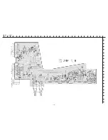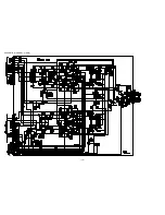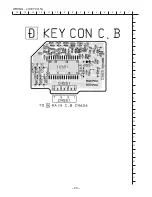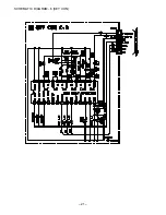
– 32 –
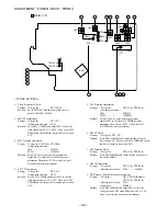
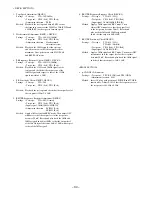
ADJUSTMENT (TUNER / DECK / FRONT)
1. Clock Frequency Check
Settings : • Test point :
TP2 (CLK)
Method : Set to MW 1602kHz and check that the test
point is 2052kHz
±
45Hz.
2. MW VT Adjustment
Settings : • Test point :
TP1 (VT)
• Adjustment location : L953
Method : Set to MW 1710kHz and adjust L953 so that the
test point become 8.3V
±
0.05V. Then set to MW
530kHz and check that the test point is more than
0.3V.
3. MW Tracking Adjustment
Settings : • Test point : TP8 (Lch), TP9 (Rch)
• Adjustment location :
L952............................... 603kHz
TC941............................ 1404kHz
Method : Set up TC941 to center before adjustment.
Adjust L952 so that level at 603kHz become
maximum. Then adjust TC941 so that the level
at 1404kHz becomes maximum.
4. SW VT Adjustment
Settings : • Test point :
TP1 (VT)
• Adjustment location : L942
Method : Set to SW 17.9MHz and adjust L942 so that the
test point becomes 8.5V
±
0.2V. Then set to SW
5.9MHz and check that the test point is more than
0.3V.
5. SW Tracking Adjustment
Settings : • Test point :
TP8 (Lch), TP9 (Rch)
• Ajustment location :
L941............................... 5.9MHz
TC943.............................17.9MHz
Method : Set up TC943 to center before adjustment.
Adjust L941 so that level at 5.9MHz becomes
maximum. Then adjust TC943 so that the level
at 17.9MHz becomes maximum.
6. FM VT Check
Settings : • Test point : TP1 (VT)
Method : Set to FM 108.0MHz and check that the test point
is less than 8.0V. Then set to FM 87.5MHz and check
that the test point is more than 0.5V.
7. FM Tracking Check
Settings : • Test point :
TP8 (Lch), TP9 (Rch)
Method : Set to FM 98.0MHz and check that the test point is
less than 9.0dB
µ
V.
8. AM IF Adjustment
Settings : • Test point :
TP8 (Lch), TP9 (Rch)
• Adjustment location : L802............450kHz
9. DC Balance / Mono Distortion Adjustment
Settings : • Test point :
TP3, TP4 (DC Balance)
TP8 (Lch), TP9 (Rch)
• Adjustment location : L801
• Input level :
60dB
µ
V
Method : Set to FM 98.0MHz and adjust L801 so that the
voltage between TP3 and TP4 becomes 0V
±
0.3V.
Next, check that the distortion is minimum.
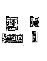
< TUNER SECTION >
TP8 (LCH)
TP9 (RCH)
IC601
L801
IC801
9
24
8
L802
TP3
TP4
TP2
(CLK)
4
L952
TP1
(VT)
FFE831
9
R815
3
7
5
3
1
2
GND
A MAIN C.B
4
L953
L942
2
6
4
5
8
9
TC941
TC943
L941
Содержание NSX-VC78
Страница 13: ... 13 SCHEMATIC DIAGRAM 1 MAIN 1 3 AMP VM ...
Страница 14: ... 14 SCHEMATIC DIAGRAM 2 MAIN 2 3 DECK HEAD 1 HEAD 2 ...
Страница 15: ... 15 SCHEMATIC DIAGRAM 3 MAIN 3 3 TUNER ...
Страница 17: ... 17 SCHEMATIC DIAGRAM 4 FRONT DECK ...
Страница 19: ... 19 SCHEMATIC DIAGRAM 5 AMP ...
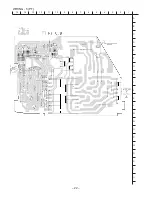
Страница 20: ...WIRING 4 KEY CON 20 1 2 3 4 5 6 7 8 9 10 11 12 13 14 15 A B C D E F G H I J K L M N O P Q R S T U ...
Страница 21: ... 21 SCHEMATIC DIAGRAM 6 KEY CON ...
Страница 22: ...WIRING 5 PT 22 1 2 3 4 5 6 7 8 9 10 11 12 13 14 15 A B C D E F G H I J K L M N O P Q R S T U ...
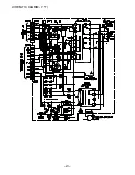
Страница 23: ... 23 SCHEMATIC DIAGRAM 7 PT ...
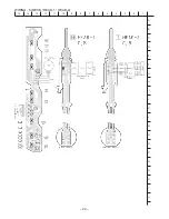
Страница 24: ...WIRING 6 DECK HEAD 1 HEAD 2 24 1 2 3 4 5 6 7 8 9 10 11 12 13 14 15 A B C D E F G H I J K L M N O P Q R S T U ...
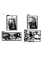
Страница 25: ... 25 IC BLOCK DIAGRAM ...
Страница 26: ... 26 ...
Страница 27: ... 27 ...
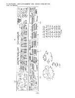
Страница 28: ... 28 FL BJ754GNK GRID ASSIGNMENT AND ANODE CONNECTION GRID ASSIGNMENT ...
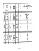
Страница 29: ... 29 ANODE CONNECTION ...
Страница 37: ... 37 TAPE MECHANISM EXPLODED VIEW 1 1 ...
Страница 41: ...2 11 IKENOHATA 1 CHOME TAITO KU TOKYO 110 JAPAN TEL 03 3827 3111 Printed in Singapore 9301978 0251431 ...

