background image

-6-

In such a case, check also if the POWER AMPLIFIER circuit or power supply circuit has any abnormalities or not.

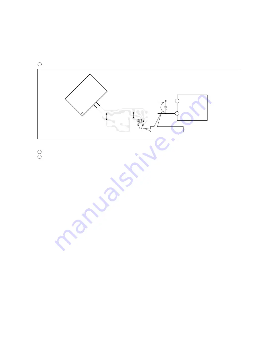
2-2. Regarding reset

There are cases that the machine does not work correctly because the MICROCOMPUTER is not reset even though the AC power cord is
re-inserted, or the software reset (pressing the STOP key + POWER key) is performed.
When the above described phenomenon occurs, it can lead to wrong judgement as if the MICROCOMPUTER is defective and to exchange the
MICROCOMPUTER. In such a case, perform the forced-reset by the following procedure and check good or no good of the MICROCOM
PUTER.
  1   Remove the AC power cord.

  2   Short both ends of the electrolytic capacitor C113 that is connected to VDD of the MICROCOMPUTER with tweezers.
  3   Connect the AC power cord again. If the MICROCOMPUTER returns to the normal operation, the MICROCOMPUTER is good.

Note: The reference number or MICROCOMPUTER pin number of transistor (Q110) and electrolytic capacitor (C113) can change depending on the

          models. Be sure to check the reference numbers on schematic diagram before starting the discharging work.

2-3. Confirmation of soldering state of MICROCOMPUTER

Check the soldering state of the MICROCOMPUTER in addition to the above described procedures. Be sure to exchange the
MICROCOMPUTER after surely confirming that the trouble is not caused by poor soldering but the MICROCOMPUTER itself.

NOTE ON BEFORE STARTING REPAIR -2/2

Fig-2-2

MICRO-
COMPUTER

MICR

OCOMPUTER

FRONT C.B

FRONT C.B

VSS

VDD

C113

16

15

C113

18

15

Short with tweezers.

Содержание NSX-R17

Страница 1: ...N6 EZ B BASIC CD MECHANISM BZG 2 ZD9GNC2 BASIC TAPE MECHANISM CMAT6Z2 1 1 ALPS If requiring information about the CD mechanism see Service Manual of BZG 2 ZD9GNC2 S M Code No 09 023 353 2NA NSX R17 SPEAKER SYSTEM CD CASSEIVER SX NR17 CX NR17 REMOTE CONTROLLER RC CAS03 VS ...

Страница 2: ...ATIC DIAGRAM 4 5 FRONT DECK SECTION 27 WIRING 2 4 FRONT C B 28 WIRING 3 4 DECK C B 29 SCHEMATIC DIAGRAM 5 5 PT SECTION 30 WIRING 4 4 PT C B 31 ELECTRICAL ADJUSTMENT 32 38 CD TEST MODE 39 FL DISPLAY HUA 13SS09T 40 IC BLOCK DIAGRAM 41 42 IC DESCRIPTION 43 44 MECHANICAL EXPLODED VIEW 45 MECHANICAL PARTS LIST 46 COLOR NAME TABLE 47 TAPE MECHANISM EXPLODED VIEW CMAT6Z2 1 1 ALPS 48 TAPE MECHANISM PARTS ...

Страница 3: ... VIDEO AUX 500 mV Outputs SPEAKERS 6 ohms or more PHONES 32 ohms or more CASSETTE DECK Track format 4 tracks 2 channels stereo Frequency response 50 Hz 15 kHz Recording system AC bias Heads DECK 1 playback x 1 DECK 2 recording playback x 1 erase x 1 CD PLAYER Laser Semiconductor laser λ 780 nm D A converter 1 bit dual Signal to noise ratio 85 dB 1 kHz 0 dB Harmonic distortion 0 05 1 kHz 0 dB GENER...

Страница 4: ... osynling laserstrålning som överskrider gränsen för laserklass 1 PROTECTION OF EYES FROM LASER BEAM DURING SERVICING 1 1 CAUTION Use of controls or adjustments or performance of proce dures other than those specified herin may result in hazardous radiation exposure ATTENTION L utillisation de commandes réglages ou procédures autres que ceux spécifiés peut entraîner une dangereuse exposition aux r...

Страница 5: ...e models Be sure to check the reference numbers of the charging capacitors on schematic diagram before starting the discharging work 2 Check items before exchanging the MICROCOMPUTER Be sure to check the following items before exchanging the MICROCOMPUTER Exchange the MICROCOMPUTER after confirming that the MICROCOMPUTER is surely defective 2 1 Regarding the HOLD terminal of the MICROCOMPUTER When...

Страница 6: ... capacitor C113 that is connected to VDD of the MICROCOMPUTER with tweezers 3 Connect the AC power cord again If the MICROCOMPUTER returns to the normal operation the MICROCOMPUTER is good Note The reference number or MICROCOMPUTER pin number of transistor Q110 and electrolytic capacitor C113 can change depending on the models Be sure to check the reference numbers on schematic diagram before star...

Страница 7: ... parts for service and will be stocked at the spare parts centers Components marked X and R are not designated as spare parts for after sales service and will not be stocked at the spare parts centers UNIT NAME C REF NO PARTS NO PARTS NAME SUFFIX MODEL 7 ACCESSORIES PARTS LIST 1 1 CX SNR17 EZBC1 O AS1001 8C NFA 916 110 IB EZ 9L S NSX R10 a O AS1002 8C NF8 702 110 RC UNIT RC CAS03 VS a O AS1003 87 ...

Страница 8: ... 274 080 C CAP U 1000P 50 K B GRM a FRONT O C 0912 87 010 759 080 C CAP U 0 1 25 Z F CM CB a FRONT O C 0913 87 A10 189 040 CAP E 220 10 M 5L a FRONT O C 0915 87 010 759 080 C CAP U 0 1 25 Z F CM CB a FRONT O C 0916 87 010 759 080 C CAP U 0 1 25 Z F CM CB a FRONT O C 0917 87 010 759 080 C CAP U 0 1 25 Z F CM CB a FRONT O C 0919 87 012 286 080 C CAP U 0 01 25 K B GRM a FRONT O C 0920 87 010 829 080 ...

Страница 9: ... 8K 1 16W J a FRONT X R 0328 88 121 182 080 RES 1 8K 1 8W J a FRONT O R 0329 88 108 272 080 C RES U 2 7K 1 16W J a FRONT O R 0330 88 108 332 080 C RES U 3 3K 1 16W J a FRONT X R 0331 88 121 472 080 RES 4 7K 1 8W J a FRONT X R 0332 88 108 682 080 C RES U 6 8K 1 16W J a FRONT O R 0333 88 108 103 080 C RES U 10K 1 16W J a CX SNR17 EZBC1 FRONT X R 0334 88 108 183 080 C RES U 18K 1 16W J a FRONT O R 03...

Страница 10: ... RES U 100K 1 16W J a FRONT O R 0822 88 108 224 080 C RES U 220K 1 16W J a FRONT X R 0823 88 100 000 010 PLATING JW 0 58 SN95 a FRONT X R 0824 88 100 000 010 PLATING JW 0 58 SN95 a FRONT X R 0825 88 100 000 010 PLATING JW 0 58 SN95 a FRONT X R 0826 88 108 000 080 C JUMPER U a FRONT O R 0827 88 108 473 080 C RES U 47K 1 16W J a CX SNR17 EZBC1 FRONT X R 0901 88 108 104 080 C RES U 100K 1 16W J a FRO...

Страница 11: ...RONT O S 0331 87 A90 164 080 SW TACT SKQNAB N a FRONT O S 0332 87 A90 164 080 SW TACT SKQNAB N a FRONT O S 0333 87 A90 164 080 SW TACT SKQNAB N a FRONT O S 0334 87 A90 164 080 SW TACT SKQNAB N a FRONT O S 0335 87 A90 164 080 SW TACT SKQNAB N a FRONT O S 0341 87 A90 164 080 SW TACT SKQNAB N a CX SNR17 EZBC1 FRONT O S 0342 87 A90 164 080 SW TACT SKQNAB N a FRONT O S 0343 87 A90 164 080 SW TACT SKQNA...

Страница 12: ...0 C CAP U 0 1 25 Z F CM CB a MAIN O C 0451 87 010 759 080 C CAP U 0 1 25 Z F CM CB a MAIN O C 0452 87 010 406 080 CAP E 22 50 M 11L SME a MAIN O C 0453 87 012 279 080 C CAP U 2700P 50 K B GRM a MAIN O C 0454 87 012 279 080 C CAP U 2700P 50 K B GRM a MAIN O C 0455 87 012 279 080 C CAP U 2700P 50 K B GRM a MAIN O C 0456 87 012 286 080 C CAP U 0 01 25 K B GRM a CX SNR17 EZBC1 MAIN X C 0457 88 708 730...

Страница 13: ...L SME a MAIN O C 0810 87 010 759 080 C CAP U 0 1 25 Z F CM CB a MAIN O C 0814 87 012 286 080 C CAP U 0 01 25 K B GRM a MAIN O C 0815 87 010 400 080 CAP E 0 47 50 M 11L SME a MAIN O C 0816 87 010 400 080 CAP E 0 47 50 M 11L SME a MAIN O C 0818 87 012 276 080 C CAP U 1500P 50 K B GRM a MAIN O C 0821 87 010 405 080 CAP E 10 50 M 11L SME a MAIN X C 0822 88 108 000 080 C JUMPER U a CX SNR17 EZBC1 MAIN ...

Страница 14: ...P U 1000P 50 K B GRM a MAIN O C 0997 87 010 759 080 C CAP U 0 1 25 Z F CM CB a MAIN O C 0998 87 010 260 080 CAP E 47 25 M 11L SME a MAIN O C 0999 87 A11 155 080 CAP TC U 0 01 16 Z F a MAIN O CF 0831 87 008 423 010 FLTR CF SFE10 7MS3G A a MAIN O CF 0832 82 785 747 010 CF MS2GH A a MAIN X CLP0303 87 A60 884 010 PIN DIA1 COATING SHS a MAIN X CLP0304 87 A60 884 010 PIN DIA1 COATING SHS a MAIN O CN 030...

Страница 15: ...L 0905 86 ZA1 613 010 COIL FM ANT RF 2 Z a MAIN O L 0906 87 005 847 080 COIL 2 2UH K CECS a MAIN O L 0907 86 ZA1 614 010 COIL FM OSC Z a MAIN O L 0908 88 ZA1 624 010 COIL FM IFT 7 6 2 COILS a MAIN O L 0941 87 A50 020 010 COIL ANT LW COI 252KHZ a MAIN O L 0942 87 A50 019 010 COIL OSC LW COI 856KHZ a MAIN O L 0952 87 A50 754 010 COIL MW ANT 3BLW a MAIN O L 0953 87 A50 755 010 COIL MW OSC 3BLW a MAIN...

Страница 16: ...3 080 C RES U 22K 1 16W J a MAIN X R 0011 88 108 472 080 C RES U 4 7K 1 16W J a MAIN X R 0012 88 118 472 080 C RES S 4 7K 1 10W J a MAIN X R 0013 88 118 472 080 C RES S 4 7K 1 10W J a MAIN X R 0014 88 118 100 080 C RES S 10 1 10W J a MAIN X R 0015 88 108 104 080 C RES U 100K 1 16W J a CX SNR17 EZBC1 MAIN X R 0016 88 108 104 080 C RES U 100K 1 16W J a MAIN X R 0017 88 108 104 080 C RES U 100K 1 16W...

Страница 17: ...8 472 080 C RES U 4 7K 1 16W J a MAIN O R 0159 88 108 103 080 C RES U 10K 1 16W J a MAIN X R 0160 88 118 103 080 C RES S 10K 1 10W J a MAIN X R 0165 88 118 152 080 C RES S 1 5K 1 10W J a MAIN X R 0166 88 118 152 080 C RES S 1 5K 1 10W J a MAIN O R 0167 88 108 103 080 C RES U 10K 1 16W J a MAIN X R 0168 88 118 473 080 C RES S 47K 1 10W J a CX SNR17 EZBC1 MAIN X R 0171 88 118 222 080 C RES S 2 2K 1 ...

Страница 18: ...6W J a MAIN O R 0626 88 108 103 080 C RES U 10K 1 16W J a MAIN X R 0627 88 108 222 080 C RES U 2 2K 1 16W J a MAIN X R 0628 88 108 222 080 C RES U 2 2K 1 16W J a MAIN O R 0629 88 108 103 080 C RES U 10K 1 16W J a MAIN O R 0630 88 108 103 080 C RES U 10K 1 16W J a MAIN X R 0631 88 108 222 080 C RES U 2 2K 1 16W J a MAIN X R 0632 88 108 222 080 C RES U 2 2K 1 16W J a CX SNR17 EZBC1 MAIN X R 0633 88 ...

Страница 19: ...88 108 472 080 C RES U 4 7K 1 16W J a MAIN X R 0915 88 108 104 080 C RES U 100K 1 16W J a MAIN X R 0916 88 108 470 080 C RES U 47 1 16W J a MAIN O R 0926 88 108 101 080 C RES U 100 1 16W J a MAIN O R 0944 88 108 101 080 C RES U 100 1 16W J a MAIN X R 0945 88 108 104 080 C RES U 100K 1 16W J a MAIN X R 0947 88 108 183 080 C RES U 18K 1 16W J a CX SNR17 EZBC1 MAIN X R 0948 88 108 472 080 C RES U 4 7...

Страница 20: ...C NF9 619 010 SHLD CASE CNF 9 EZ P a MAIN O TC 0942 87 A91 774 080 TRIMMER PLY 30P 6 8X5 4 CDYL a MAIN O TH 0101 87 A91 042 080 C THMS 100K 55001 a MAIN O TH 0102 87 A91 042 080 C THMS 100K 55001 a MAIN O W 0099 8C NFA 605 010 F CABLE 5P 2 5 480MM a MAIN O W 0101 8B NF1 640 010 F CABLE 5P 2 5 250MM a MAIN O WH 0001 87 A90 459 010 HLDR WIRE 2 5 5P a MAIN O WH 0101 87 A90 459 010 HLDR WIRE 2 5 5P a ...

Страница 21: ... 0 8 0 45 2 1 25 0 45 3 2 1 6 108 118 128 A A CHIP RESISTOR PART CODE 0 55 Resistor Code Dimensions mm Symbol 1 16W 1005 5 CJ 1 0 0 5 0 35 104 L t W Regarding connectors they are not stocked as they are not the initial order items The connectors are available after they are supplied from connector manufacturers upon the order is received 21 ELECTRICAL PARTS LIST 14 14 ...

Страница 22: ... 2SA1980G 2SA1981Y 2SC3331 T U 2SA1585SR E C B E C B 2SC5343GL B C E S D G 2SJ460 2SK2541 E B C 2SA1235F 2SC2620B 2SC3052F 2SC3906KR 2SC5345SF S O 2SC5477 2SD1306NE07TL SRA2202S SRA2207S 2SB1342 2SB1370E 2SD1933 S 2SK360E G D D 2SK2158 S G ...

Страница 23: ... 23 SCHEMATIC DIAGRAM 1 5 MAIN 1 2 AMP SECTION NC NC NC SH301 PLATE SHLD DECK M 2SB1370E 2SD1306 NE07TL 2SD1306 NE07TL MAIN C B 1 2 AMP SECTION CLP303 PIN DIA1 COATING SHS CLP304 PIN DIA1 COATING SHS ...

Страница 24: ... 24 SCHEMATIC DIAGRAM 2 5 MAIN 2 2 TUNER SECTION MAIN C B 2 2 TUNER SECTION 1K R789 33K 2SC5477 SH901 SHLD CASE CNF 9 EZ P ...

Страница 25: ... 25 SCHEMATIC DIAGRAM 3 5 HP SECTION TO MAIN C B 1 2 AMP SECTION WH101 ...

Страница 26: ... C917 R909 C789 Q304 Q309 Q308 Q305 C612 R632 C465 R627 Q451 R302 C614 SFR451 R457 C464 R601 Q302 C607 R603 C603 R997 R995 R990 C997 R993 R998 SFR452 CLP303 CLP304 COAXIAL 10 11 12 13 14 15 16 17 18 19 20 21 22 23 24 A B C D E F G H I J K L M N O P Q R S T U 1 2 3 4 5 6 7 8 9 25 26 27 28 29 30 31 32 WIRING 1 4 MAIN C B HP C B 26 ...

Страница 27: ... 27 SCHEMATIC DIAGRAM 4 5 FRONT DECK SECTION NC NC NC FRONT C B DECK C B FFC103 FFC731 18K TO MAIN C B 1 2 AMP SECTION CN601 ...

Страница 28: ... FFC103 10 11 12 13 14 15 16 17 18 19 20 21 22 23 24 A B C D E F G H I J K L M N O P Q R S T U 1 2 3 4 5 6 7 8 9 25 26 27 28 29 30 31 32 28 WIRING 2 4 FRONT C B ...

Страница 29: ...K WHT GRN YEL RED WHT 7 8 6 5 4 3 2 1 E E R R L L L L E RP HEAD DECK 2 P HEAD DECK 1 GRY WHT BLK RED WHT BLK RED TO MAIN C B CN302 CNA301 3 2 1 TO MAIN C B CN301 R R DECK C B 10 11 12 13 14 15 16 17 18 19 20 21 22 23 24 A B C D E F G H I J K L M N O P Q R S T U 1 2 3 4 5 6 7 8 9 25 26 27 28 29 30 31 32 ...

Страница 30: ... 30 SCHEMATIC DIAGRAM 5 5 PT SECTION TO MAIN C B 1 2 AMP SECTION WH001 ...

Страница 31: ...WIRING 4 4 PT C B 31 1 2 3 4 5 6 7 8 9 10 11 12 13 14 15 A B C D E F G H I J K L M N O P Q R S T U ...

Страница 32: ... PARTS SIDE 5 6 9 J2 0 3 5 6 7 9 L802 L952 L905 L904 R L G 15 TP8 TP9 16 17 18 19 IC801 24 1 2 4 VT GND 3 L907 L953 MAIN C B PATTERN SIDE MOTOR SFR 12 DECK C B PH 15 RPH 15 L902 L901 3 7 TC942 L941 L942 1 ELECTRICAL ADJUSTMENT 1 7 ...

Страница 33: ...r below 4 Adjust the receiving frequency of the unit to 531 kHz 5 Check that the digital multimeter indicates 0 5 V or above 3 VT Adjustment and Check FM Requirements Same as Item 1 1 Connect the digital multimeter to VT and GND 2 Set the unit function to FM and adjust the receiving frequency at 108 0 MHz 3 Adjust L907 so that the digital multimeter indicates 7 0 0 1 V 4 Adjust the receiving frequ...

Страница 34: ...um 2 Adjust the unit to MW 999 kHz 3 While monitoring the 1 kHz waveform through oscilloscope decrease the S S G output level till slight noises appear in the waveform 4 Adjust L952 so that the millivoltmeter indicates maximum 5 Adjust the S S G setting to AM carrier at 603 kHz distortion rate at 30 and source at 1 kHz 6 Adjust the unit to MW 603 kHz 7 Adjust L953 so that the millivoltmeter indica...

Страница 35: ...output at maximum 2 Adjust the unit to FM 108 MHz 3 While monitoring 1 kHz waveform through oscilloscope decrease the S S G output level till slight noises appear in the waveform 4 Adjust L905 L904 L902 L901 L902 L904 L905 Repeat adjustment L905 L904 L902 L901 two or three time so that the millivoltmeter indicates the maximum level 10 Separation Check Requirements Same as Item 9 1 Adjust the S S G...

Страница 36: ...0 and check that the level is 0 25 or below 15 Head Azimuth Adjustment DECK 1 DECK 2 Requirements Measuring instrument Oscilloscope Test tape TTA 300 10 kHz Test point TP8 Lch TP9 Rch Adjustment point Head azimuth adjustment screw 1 Connect the CH1 of the oscilloscope probe to TP8 Lch and the CH2 to TP9 Rch 2 Set the V mode of the oscilloscope to ADD 3 Insert the test tape TTA 300 to DECK 1 Playba...

Страница 37: ... 2 Connect the output terminal of oscillator to attenuator and then attenuator to AUX of the unit 3 Insert the test tape TTA 602 to DECK 2 and record the 1 kHz signal from AUX 4 Adjust the attenuator so that the output levels of TP8 and TP9 become 10 mV 5 Record 1 kHz and 8 kHz alternately 6 Adjust SFR451 Lch and SFR452 Rch so that the playback output level of 8 kHz is ranged within 0 dB 1 dB comp...

Страница 38: ...y counter Test point CLOCK GND Adjustment point L951 1 While pressing and holding down the POWER button and the UP button insert the AC plug 2 Adjust L951 so that the frequency counter indicates 72 743 0 073 Hz Hz FREQUENCY COUNTER CLOCK GND 20 L951 20 FRONT C B PATTERN SIDE FRONT C B PARTS SIDE GND KSCAN ...

Страница 39: ...utton OFF and ON is repeated by every press of the PAUSE button 5 Sled mode FF button TEST PU moves to the innermost position 3 At the same time lens is kicked Sled circuit check toward inner position Tracking circuit check RWD button TEST PU moves to the outermost position 3 Mechanism movement check At the same time lens is kicked toward PU check outer position 6 Spindle mode All lit When the but...

Страница 40: ... 40 FL DISPLAY 1 1 HUA 13SS09T GRID ASSIGNMENT ANODE CONNECTION PINCONNECTION ...

Страница 41: ... 41 IC BLOCK DIAGRAM 1 2 IC LC72131D N IC BD3881FV ...

Страница 42: ... 42 IC BLOCK DIAGRAM 2 2 IC LA1845N A ...

Страница 43: ...System power supply ON OFF output 21 I JOG_A I JOG rotary encoder signal input A D 22 I JOG_B I JOG rotary encoder signal input A D 23 I VOL_A I VOL rotary encoder signal input A D 24 I VOL_B I VOL rotary encoder signal input A D 25 I SUBQ I CD SUBQ serial input 26 I WRQ I CD IC control input 27 I DRF I CD IC control input 28 I RDS_CLK I Tuner RDS clock output for BU1920FS 29 I RDS_DATA I Tuner RD...

Страница 44: ...P16 output 71 P15 AM 10K I O FL segment P15 output AM 10K data input to diode not used 72 P14 KARAOKE I O FL segment P14 output KARAOKE data input to diode not used 73 P13 LW I O FL segment P13 output LW data input to diode 74 P12 SW I O FL segment P12 output SW data input to diode not used 75 P11 OIRT I O FL segment P11 output OIRT data input to diode not used 76 P10 FM WIDE I O FL segment P10 ou...

Страница 45: ...XPLODED VIEW 1 1 42 1 2 7 12 11 12 13 14 15 16 18 19 20 22 25 26 29 30 31 32 36 37 38 39 34 35 33 40 41 42 43 44 46 47 28 45 48 49 10 23 23 24 24 9 17 21 A A A B B B A A G F F F G C H D F F A E E I A 8 6 4 3 28 28 27 5 ...

Страница 46: ... a X MC1021 8C NFA 659 010 PWB HP RDS B F a O MC1022 87 NF4 216 010 HLDR LOCK 1 a O MC1023 86 NF9 224 010 SPR C LOCK a O MC1024 82 NF5 229 010 PLATE LOCK a X MC1025 8C NF9 201 010 PLATE EARTH MECHA a O MC1026 87 NF4 217 110 HLDR LOCK 2 a X MC1027 M8 CZK 292 170 CMAT6Z2 1 1 ALPS a O MC1028 87 A90 193 010 HLDR CV100 B a O MC1029 88 908 301 110 FF CABLE 8P 1 25 300MM a O MC1030 88 911 101 110 FF CABL...

Страница 47: ...P Pink R Red S Silver ST Titan Silver T Brown V Violet W White WT Transparent White Y Yellow YT Transparent Yellow LM Metallic Blue LL Light Blue GT Transparent Green LD Dark Blue DT Transparent Orange GM Metallic Green YM Metallic Yellow DM Metallic Orange PT Transparent Pink LA Aqua Blue GL Light Green HT Transparent Gray HM Metallic Gray NH Champagne Gold M Wood Pattern ...

Страница 48: ... 48 TAPE MECHANISM EXPLODED VIEW 1 1 CMAT6Z2 1 1 ALPS 1 6 6 3 3 10 15 11 16 17 18 19 19 18 40 41 20 22 23 39 21 25 26 27 28 29 30 31 32 33 34 35 36 37 38 24 12 13 14 7 9 8 2 5 4 ...

Страница 49: ...11 414 000 SCREW PAN SW 2 6X5 ZN a O ST1012 SF J11 131 000 PW 4 1X0 13 a O ST1013 SF J11 135 000 PW 4 1X0 25 a O ST1014 SU J16 F11 000 PW 1 75X0 4 a O ST1015 SF 514 131 000 ROLLER PINCH R BLK a O ST1016 SF 612 252 000 CHASSIS BASE BLK a O ST1017 SF 567 700 000 PWB CONTROL BLK a O ST1018 SF J11 130 000 PW 2 6X0 25 a O ST1019 SF F19 S31 000 F R BELT a O ST1020 SF R26 C11 000 ASSY F W a CMAT6Z222A O ...

Страница 50: ...l it turning to clockwise direction until click sound comes out Remove the grill frame and four pieces of rubber caps by pulling out with a flat bladed screwdriver Remove the screws from hole where installed rubber caps Insert a flat bladed screwdriver into the position indicated by the arrows and remove the panel Re move the screws of each speaker unit and then remove the speaker units TOOLS 1 Pl...

Страница 51: ...rvice and will not be stocked at the spare parts centers UNIT NAME C REF NO PARTS NO PARTS NAME SUFFIX MODEL 51 SPEAKER PARTS LIST 1 1 SX NR17 SX SNR17 YB1N O SP1001 8A NSJ 006 010 BADGE AIWA S35 a X SP1002 8C NSA 002 010 GRILLE FRAME a O SP1003 8C NSA 003 010 PANEL BA DUCT a O SP1004 8C NSA 004 010 PANEL DUCT a O SP1005 8C NSA 007 010 CORD SPKR S a O SP1006 8C NSA 020 010 CABI M a O SP1007 8C NSA...

Страница 52: ...cked at the spare parts centers UNIT NAME C REF NO PARTS NO PARTS NAME SUFFIX MODEL 52 OTHER PARTS LIST 1 1 CX SNR17 EZBC1 X 87 B40 057 010 BAG PP 0 03 150 200 a X 87 B40 098 010 BAG PV 0 025 650 750 PL a X 8C NH9 853 010 CUSHION FRONT C a X 8C NH9 854 010 CUSHION REAR C a X 92 370 716 010 SH FOAMED MAT 0 31 700 500 a X 87 B40 085 010 BAG PV 0 04 200 350 PL a X 87 B50 079 010 LIST FACILITY B 0007 ...

Страница 53: ...2 11 IKENOHATA 1 CHOME TAITO KU TOKYO 110 8710 JAPAN TEL 03 3827 3111 0251431 ...

Отзывы: