– 41 –
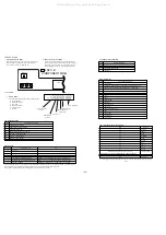
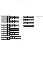
1
LOAD
O
Output terminal to loading motor rotation control.
STOP Forward Reverse Break
LOAD
L
H
L
H
2
UNLOAD
O
UNLOAD
L
L
H
H
3
S-SENS
I
Tape top direction signal. L: when detected.
4
E-SENS
I
Tape end detection signal. L: when detected.
5
SAFTY
I
Write protect/enable switch detection. L: record enable.
6
NC
–
Not used.
7~19
S0~S12
O
FDP segment signal.
20~29
T9~T0
O
FDP timing signal.
30
VFDP
–
Negative voltage (–) power supply for FDP.
31
VDD
–
Power 5V.
32
JOG VD
O
Pseudo vertical sync signal.
33
CAP LIM
O
I-LIMIT control signal output. PWM: during slowmotion mode.
34
CAP PWM
O
Capstan control PWM output.
35
DRUM PWM
O
Drum control PWM output.
36
REC–V/A
O
Video/Hi-Fi head amplifier record ON signal. H: during record.
37
HSW–A
O
H-Fi head amplifier select signal.
38
NA REC
O
Normal audio record ON signal. H: during record.
39
HSW–V
O
Video head amplifier select signal.
40
C–ROT
O
Chroma rotaion signal.
41
H–SEL
O
Video head amplifier select signal. H: when LP Head.
42
RMC OUT
O
Remote control signal output.
43
REC CTL
O
Ctl writing signal output. PULSE: during record.
44
PB CTL IN
I
CTL head pulses are input during playback.
45
DEG/PG IN
I
Drum FG/PG input.
46
RMC IN
I
Remote control signal input.
47
WAKE
I
Power failure detection input. H: power is off. L: power is on.
48
CFGA IN
I
Capstan FG-A input.
49
CFGB IN
I
Capstan FG-B input.
50
C-SYNC
I
Compositr.
51
D–ENV
I
Video head playback output comparision signal.
52
SDA–R
I/O
I2C bus data signal. (video/hifi/MPX/RF).
53
SCL–R
O
I2C bus clock signal. (video/hifi/MPX/RF).
54
SDA–T
I/O
I2C bus data signal. (canal/tuner/vps.pdc/E2PROM).
55
SCL–T
O
I2C bus clock signal. (canal/tuner/vps.pdc/E2PROM).
56~58
KEY IN 1~3
I
Key read-out A/D input.
59
A LEVEL
I
Hi-Fi envelope detection input. (Analog input).
60
V LEVEL
I
Video envelope detection input for audio tracking (Analog input).
61
AFT
I
AFT voltage read-out A/D input.
62
AGC
I
AGC voltage read-out A/D input.
Description
Pin No.
Pin Name
I/O
IC DESCRIPTION
IC, TMP93CW76F-1A78,TMP93CW76F-1A77
I/O
Description
Pin No.
Pin Name
63
DEC
I
CANAL decoder detection input. L: when detected.
64
ADGND
–
A/D GND
65
ADREF
–
A/D reference voltage.
66
SPDATA
I
Serial data signal from TC4021.
67
TXD
O
Serial data signal for TC4094 & OSD IC.
68
CLK
O
Serial clock signal for communication with TC4094 and OSD.
69
T–REEL
I
Take up reel rotation detection input.
70
S–REEL
I
Supply reel rotation detection input.
71
XT/2
O
Terminal for check of system clock.
72
GND
–
GND.
73
X1
–
External 16MHz crystal for main clock is connected to this terminal.
74
X2
–
75
Not use
–
Connetcted to power supply.
76
RESET
–
CPU reset input.
77
XT1
–
External 32.768 kHz crystal for sub clock is connected to this terminal.
78
XT2
–
79
TSET1
O
Connected to power TEST2.
80
TSET2
I
Connected to power TEST1.
81
NC
–
Not used.
82
SNSR CTL
O
TOP/END sensor LED drive signal.
83
STRB1
O
TC4094 chip select signal.
84
STRB2
O
TC4021 chip select signal.
85
OSD RESET
O
Reset for OSD IC signal.
86
A MUTE
O
Audio mute signal. H: mute.
87
OSD STRB
O
OSD IC chip select signal.
88
T–POWER
O
Timer power supply ON signal. L: power off. H: power on.
89
P–BU
O
RF power supply ON signal. L: power off. H: power on.
90
P–ON
O
REG power supply ON signal. L: power off. H: power on.
91
P–CA
O
CANAL power supply ON signal. L: power off. H: power on.
92
M–PRT
I
Motor-power monitoring input.
93
P–STBY
O
Power supply control signal. STBY5V.
94
CAP RVS
O
Capstan inverted signal. L: normal rotation. H: reverse rotation.
95
PCBTEST
I
Test mode starting up input.
96
CAON
I
Picture input from TV detection input during save mode.
97
HF DET
I
Hi-Fi detection signal input. L: whwn detected.
98~100
CAM C, B, A
I
Mechanism mode switch C, B, A.
All manuals and user guides at all-guides.com
all-guides.com
Содержание HV-FX8700
Страница 3: ...3 All manuals and user guides at all guides com...
Страница 12: ...12 C WIRE HARNESS DIAGRAM All manuals and user guides at all guides com...
Страница 13: ...BLOCK DIAGRAM 1 SYSCON SERVO 13 All manuals and user guides at all guides com...
Страница 14: ...BLOCK DIAGRAM 2 VIDEO 14 All manuals and user guides at all guides com...
Страница 15: ...BLOCK DIAGRAM 3 HIFI THEATRE 15 NOT USE WIDE WIDE All manuals and user guides at all guides com...
Страница 16: ...16 BLOCK DIAGRAM 4 TUNER All manuals and user guides at all guides com a l l g u i d e s c o m...
Страница 17: ...17 BLOCK DIAGRAM 5 MPX All manuals and user guides at all guides com...
Страница 18: ...BLOCK DIAGRAM 6 CANAL 18 SWITCH Q610 WIDE All manuals and user guides at all guides com...
Страница 19: ...19 BLOCK DIAGRAM 7 POWER PS All manuals and user guides at all guides com...
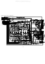
Страница 22: ...22 SCHEMATIC DIAGRAM 2 MAIN 2 4 VIDEO SECTION All manuals and user guides at all guides com...
Страница 23: ...23 SCHEMATIC DIAGRAM 3 MAIN 3 4 HIFI SECTION All manuals and user guides at all guides com...
Страница 25: ...25 SCHEMATIC DIAGRAM 4 FR1 FR2 All manuals and user guides at all guides com...
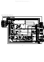
Страница 27: ...27 SCHEMATIC DIAGRAM 6 REAR 2 2 CANAL SECTION All manuals and user guides at all guides com...
Страница 29: ...29 SCHEMATIC DIAGRAM 7 TUNER All manuals and user guides at all guides com...
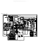
Страница 30: ...30 SCHEMATIC DIAGRAM 8 MAIN 4 4 POWER SECTION All manuals and user guides at all guides com...
Страница 31: ...31 SCHEMATIC DIAGRAM 9 PS All manuals and user guides at all guides com a l l g u i d e s c o m...
Страница 32: ...32 SCHEMATIC DIAGRAM 10 MPX All manuals and user guides at all guides com...
Страница 38: ...38 IC BLOCK DIAGRAM All manuals and user guides at all guides com...

