background image

Preface

 iii

EGX-MXM-P2000

Preface

Copyright © 2019 ADLINK Technology Inc.

This document contains proprietary information protected by copy-
right. All rights are reserved. No part of this manual may be repro-
duced by any mechanical, electronic, or other means in any form
without prior written permission of the manufacturer.

Disclaimer

The information in this document is subject to change without prior
notice in order to improve reliability, design, and function and does
not represent a commitment on the part of the manufacturer.

In no event will the manufacturer be liable for direct, indirect, spe-
cial, incidental, or consequential damages arising out of the use or
inability to use the product or documentation, even if advised of
the possibility of such damages.

Environmental Responsibility

ADLINK is committed to fulfill its social responsi-
bility to global environmental preservation through
compliance with the European Union's Restriction
of Hazardous Substances (RoHS) directive and
Waste Electrical and Electronic Equipment
(WEEE) directive. Environmental protection is a
top priority for ADLINK. We have enforced mea-
sures to ensure that our products, manufacturing
processes, components, and raw materials have
as little impact on the environment as possible. When products are
at their end of life, our customers are encouraged to dispose of
them in accordance with the product disposal and/or recovery pro-
grams prescribed by their nation or company.

Battery Labels 

(for products with battery)

ᘄ㟁ụㄳᅇᨲ

Содержание EGX-MXM-P2000

Страница 1: ...Leading EDGE COMPUTING EGX MXM P2000 NVIDIA Pascal GP107 Quadro P2000 Embedded Graphics Module User s Manual Manual Rev 1 0 Revision Date November 21 2019 Part No 50 1Z300 1000...

Страница 2: ...ii Revision History Leading EDGE COMPUTING Revision History Revision Release Date Description of Change s 1 0 2019 11 21 Initial release...

Страница 3: ...ut of the use or inability to use the product or documentation even if advised of the possibility of such damages Environmental Responsibility ADLINK is committed to fulfill its social responsi bility...

Страница 4: ...harm For more information go to www P65Warnings ca gov Trademarks Product names mentioned herein are used for identification pur poses only and may be trademarks and or registered trademarks of their...

Страница 5: ...isplay Support and Options 3 1 3 4 OS Support 3 1 3 5 Software Support 3 1 3 6 Graphics Options 4 1 4 Functional Block Diagram 5 1 5 Layout and I O 6 1 5 1 MXM Connector Pin Definition 8 1 6 Thermal P...

Страница 6: ...vi Table of Contents Leading EDGE COMPUTING 2 7 Certifications Agencies 19 Important Safety Instructions 21 Getting Service 23...

Страница 7: ...e 1 1 Board Specifications 2 Table 1 2 Memory Configuration 3 Table 1 3 Display Support and Options 3 Table 1 4 Graphics Module Display Options 4 Table 1 5 NVIDIA Link Display Types 4 Table 1 6 MXM Co...

Страница 8: ...viii List of Tables Leading EDGE COMPUTING This page intentionally left blank...

Страница 9: ...igure 1 2 MXM Module Basic Dimensions 6 Figure 1 3 MXM Module Detailed Dimensions and Layout 7 Figure 2 1 Power Sequencing 15 Figure 2 2 Module Power Down 16 Figure 2 3 Reset Sequencing 16 Figure 2 4...

Страница 10: ...x List of Figures Leading EDGE COMPUTING This page intentionally left blank...

Страница 11: ...module supports operability in an extended temper ature range of 40 C to 85 C suitable for mission critical harsh environments With its 768 CUDA core Pascal GPU the EGX MXM P2000 supports 4 FHD displ...

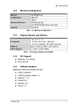
Страница 12: ...t color depth Signal Interface MXM 3 1 PCI Express Gen3 x16 support GPGPU Computing CUDA Support 768 CUDA cores 2 3TFLOPS SP Peak CUDA Toolkit 8 0 CUDA Compute version 6 1 OpenCL 1 2 DirectX 12 OpenGL...

Страница 13: ...Supported software packages include X CUDA Toolkit 8 0 X CUDA Compute version 6 1 X OpenCL 1 2 X DirectX 12 X OpenGL 4 5 X Vulcan 1 0 Memory GDDR5 6Gbps Configuration 256Mx32 Memory Bandwidth 128 bit...

Страница 14: ...own Table 1 4 Graphics Module Display Options Table 1 5 NVIDIA Link Display Types Item Detail MXM Port DP_A DP_B DP_C DP_D NVIDIA Link Link E Link F Link A Link B Link Display Type Link A DisplayPort...

Страница 15: ...P1 4 DP1 4 PCIE x16 Gen3 I2CS PM JTAG SPI SPI VBIOS MXM 3 1 Connector P SRC P 5V P 3V3 SPI JTAG I2CS GDDR5 x32 memory down GDDR5 x32 memory down GDDR5 x32 memory down GDDR5 x32 memory down GDDR5 Chann...

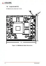
Страница 16: ...6 Introduction Leading EDGE COMPUTING 1 5 Layout and I O All dimensions shown are in mm Figure 1 2 MXM Module Basic Dimensions 82 70 3 2 0 x 6 6 x 6...

Страница 17: ...Introduction 7 EGX MXM P2000 Figure 1 3 MXM Module Detailed Dimensions and Component Layout 0 1 3 6...

Страница 18: ...LVDS_U_HPD NI 15 GND 16 JTAG_TESTEN 17 GND 18 PWR_LEVEL 100K PU 3 3V 19 PEX_STD_SW NI 20 TH_OVERT 100K PU 3 3V 21 VGA_DISABLE NI 22 TH_ALERT 100K PU 3 3V 23 PNL_PWR_EN 24 TH_PWM NI 25 PNL_BL_EN 26 GP...

Страница 19: ...72 PEX_TX11 73 PEX_RX11 74 PEX_TX11 75 PEX_RX11 76 GND 77 GND 78 PEX_TX10 79 PEX_RX10 80 PEX_TX10 81 PEX_RX10 82 GND 83 GND 84 PEX_TX9 85 PEX_RX9 86 PEX_TX9 87 PEX_RX9 88 GND 89 GND 90 PEX_TX8 91 PEX...

Страница 20: ...PEX_RX2 136 PEX_TX2 137 PEX_RX2 138 PEX_TX2 139 GND 140 GND 141 PEX_RX1 142 PEX_TX1 143 PEX_RX1 144 PEX_TX1 145 GND 146 GND 147 PEX_RX0 148 PEX_TX0 149 PEX_RX0 150 PEX_TX0 151 GND 152 GND 153 PEX_REF...

Страница 21: ...190 LVDS_LTX2 NI 191 GND 192 GND 193 LVDS_UTX0 NI 194 LVDS_LTX1 NI 195 LVDS_UTX0 NI 196 LVDS_LTX1 NI 197 GND 198 GND 199 DP_C_L0 200 LVDS_LTX0 NI 201 DP_C_L0 202 LVDS_LTX0 NI 203 GND 204 GND 205 DP_C...

Страница 22: ...D 250 GND 251 GND 252 DP_B_L1 253 DP_A_L0 254 DP_B_L1 255 DP_A_L0 256 GND 257 GND 258 DP_B_L2 259 DP_A_L1 260 DP_B_L2 261 DP_A_L1 262 GND 263 GND 264 DP_B_L3 265 DP_A_L2 266 DP_B_L3 267 DP_A_L2 268 GN...

Страница 23: ...king materials for inspection Obtain authorization from your dealer before returning any product to ADLINK Ensure that the fol lowing items are included in the package X EGX MXM P2000 GPU module Param...

Страница 24: ...14 Introduction Leading EDGE COMPUTING This page intentionally left blank...

Страница 25: ...000 2 System Requirements 2 1 Power Sequencing For initial power on or to resume from S3 and S4 this sequence must be followed Figure 2 1 Power Sequencing TPV PE 0m s TPE PG 90m s PWR_SRC 5V 3V3 Modul...

Страница 26: ...whether to keep the module input power when the MXM module is powered down Figure 2 2 Module Power Down 2 3 Reset Requirements Figure 2 3 Reset Sequencing Module Input Power PWR_EN Module Internal Po...

Страница 27: ...upport and Options on page 3 The system requires a switch circuit to determine whether the AUX or DDC signal is output from the MXM module and AC coupling capacitors should be placed on the sys tem bo...

Страница 28: ...equired on the system board are as shown 499 with 1 pulldown resistors to the ground on the DP lanes must placed on the DVI HDMI connector side of the AC cou pling gated by a MOSFET to limit leakage F...

Страница 29: ...e downloaded from https www nvidia com tw Download index aspx 2 7 Certifications Agencies X Windows Hardware Quality Lab WHQL certified Windows 7 and Windows 10 X EU Reduction of Hazardous Substances...

Страница 30: ...20 System Requirements Leading EDGE COMPUTING This page intentionally left blank...

Страница 31: ...mperature of 50 C X When installing mounting or uninstalling removing device or when removal of a chassis cover is required for user ser vicing Z Turn off power and unplug any power cords cables Z Rei...

Страница 32: ...ns of breakage X Disconnect the power supply cord before loosening the thumbscrews and always fasten the thumbscrews with a screwdriver before starting the system up X It is recommended that the devic...

Страница 33: ...408 360 0200 Toll Free 1 800 966 5200 USA only Fax 1 408 360 0222 Email info adlinktech com ADLINK Technology China Co Ltd 300 Fang Chun Rd Zhangjiang Hi Tech Park Pudong New Area Shanghai 201203 Chi...

Отзывы: