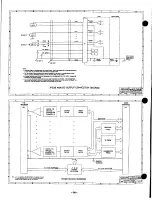
SERIES IP220 INDUSTRIAL I/O PACK
1
2
-BIT HIGH-DENSITY ANALOG OUTPUT MODULE
Power Supply
Selection•
J1
(1&2)
J1
(2&3)
J2
(1&2)
J2
(2&3)
±12 Volt (Internal, P1)
IN
OUT
IN
OUT
±15 Volt (External, P2)
OUT
IN
OUT
IN
Analog Output Voltage
(Volts)
BOB Data
(Hex)
9.9951
FFFO
9.9902
FFEO
.
.
0.0049
8010
0.0000
8000
-0.0049
7FF0
.
.
-9.9951
0010
-10.0000
0000
Pin Description Number
Pin Description
Number
+CHOO
1
-CH121
26
-CH001
2
+CH13
27
+CH01
3
-CH131
28
-CH011
4
+CH14
29
+CH02
5
-CH14'
30
-CH021
6
+CH15
31
+CH03
7
-CH151
32
-CH031
8
RESERVED
33
+CH04
9
RESERVED
34
-CH041
10
RESERVED
35
+CH05
11
RESERVED
36
-CH05'
12
RESERVED
37
+CHO6
13
RESERVED
38
-CH06'
14
RESERVED
39
+CH07
15
RESERVED
40
-CH07'
16
RESERVED
41
+CHO8
17
RESERVED
42
-CH081
18
COMMON'
43
+CH09
19
COMMON'
44
-CH09'
20
RESERVED
45
+CH10
21
RESERVED
46
-CH101
22
-15V DC
47
+CH11
23
RESERVED
48
-CH11'
24
+15V DC
49
+CH12
25
SHIELD
50
Note: 1 . T h e minus leads of all channels are connected to analog
rise above the maximum operating temperature and to prolong the
life of the electronics. I f the installation is in an industrial
environment and the board is exposed to environmental air, careful
consideration should be given to air-filtering.
BOARD CONFIGURATION
The board may be configured differently, depending on the
application. All possible jumper settings will be discussed in the
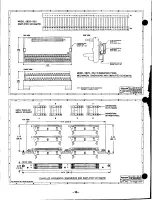
following sections. The jumper locations are shown in Drawing
4501-441.
Power should be removed from the board when configuring
hardware jumpers, installing IP modules, cables, termination panels,
and field wiring. Refer to Mechanical Assembly Drawing 4501-434
and your IP module documentation for configuration and assembly
instructions.
Default Hardware Jumper Configuration
A board is shipped from the factory configured as follows:
• I n t e r n a l ±12 Volt power supplies are used (sourced from P1).
• A n a l o g output range is -10 to +10 Volts and is not configurable.
• Programmable software register bits are undefined at reset, but
the board defaults to 0 Volts on all analog outputs and the
Simultaneous Channel Update Mode (see Section 3).
Power Supply Hardware Jumper Configuration
Hardware jumpers J1 & J2 allow the selection of internal or
external analog power supplies. J1 (J2) controls the selection of
either the in12 (-12) Volt supply sourced from the P1
connector, or the ex15 (-15) Volt supply sourced from the P2
connector. The IN/OUT configuration of the jumpers for the
different supplies is shown in the following table. "IN" means that
the pins noted are shorted together with a shorting clip. "OUT"
means that the clip has been removed.
Table 2.1: Power Supply Selections (Pins of J1 and J2
• D o not mix internal and external supplies (e.g. do not use +12V
internal with -15V external). Note that the IP220 module can
achieve rated output using either internal or external supplies.
Programmable Register Configuration
Programmable registers are software configurable. That is,
there are no hardware jumpers associated with them. Registers
must be accessed to select the desired mode of operation and to
update analog outputs (refer to Section 3 for details).
Analog Output Data Format
The bipolar output range (-10 to +10 Volts) is programmed with
Bipolar Offset Binary (BOB) data to the Digital-to-Analog-Converter
(DAC). The following table indicates the relationship between the
data format and the ideal analog output voltage from the module.
Table 2.2: Bipolar
Offset Binary (BOB) Output Data Format*
The BOB, 12-bit data is left-justified within the 16-bit word. The 4
Least Significant Bits (LSB's) are shown as zero in the table, but
actually it does not matter what is written to them.
CONNECTORS
IP Field I/O Connector (P2)
P2 provides the field I/O interface connector for mating IP
modules to the carrier board. P2 is a 50-pin receptacle female
header (AMP 173279-3 or equivalent) which mates to the male
connector of the carrier board (AMP 173280-3 or equivalent). This
provides excellent connection integrity and utilizes gold-plating in the
mating area. Threaded metric M2 screws and spacers are supplied
with the module to provide additional stability for harsh environments
(see Mechanical Assembly Drawing 4501-434). The field and logic
side connectors are keyed to avoid incorrect assembly. P2 Pin
assignments are unique to each IP (see Table 2.3) and normally
correspond to the pin numbers of the front panel, field I/O interface
connector on the carrier board (you should verify this for your carrier
board). In Table 2.3, channel designations are abbreviated to save
space (i.e. channel 0 is abbreviated as "+CHOO" & "-CHOO" for the +
& - connections, respectively). Further, note the output signals all
have the same ground reference ("-CHOO" and the minus leads of all
other channels are connected to analog common on the module).
Table 2.3: IP220 Field I/O Pin Connections (P2)
common on the module.
- 4 -


