background image

Series AVME9125                                                                                                     VMEbus 6U Analog Input Board
___________________________________________________________________________________________

- 17 -

Programmable Calibration Voltages

Calibration

Signal

Ideal

Value

(Volts)

Maximum Temperature

Drift

2

 (ppm/oC)

Auto Zero

0.0000

N/A

CAL

9.790039

±

6

Note 2.   Worst case temperature drift of the calibration voltage
reference.

Maximum Overall Calibrated Error @ 25

°

C

The maximum corrected (i.e. calibrated) error is the worst case
accuracy possible.  It is the sum of error components due to ADC
quantization of the low and high calibration signals,
Instrumentation Amp and ADC linearity error, and the absolute
errors of the recommended calibration voltages at 25oC.

Input

 Range

(Volts)

Max. Err


±

LSB

(% Span)

Typ. Er

3


±

LSB

(% Span)

-10 to +10

±

8.8 LSB

(

±

0.0113%)

±

3 LSB

(

±

.0.0045%)

Note 3.   A total of 256 input samples, were averaged with the
throughput Rate of 31KHz conversions/second.  A 3 foot shielded
analog input ribbon was used.

Settling Time (20V step)........….....3.5uS to 0.01%, Typical
A/D Conversion Time.................….11.25uS Maximum
Conversion Rate..........................…88.8KHz Maximum
A/D Triggers............................…....Software and External
Input Noise...........................….......1.4 LSB rms, Typical

4

.

Temperature Coefficient..........…....See spec of calibration
voltages.

Note 4.   A total of 2048 input samples were averaged with the
throughput Rate of 31KHz conversions/second, using the uniform
single sample mode.  A 3 foot shielded analog input ribbon was
used.

ENVIRONMENTAL

Operating Temperature..........….0 to +70

°

C

Relative Humidity........................5-95% non-condensing.  The
                                                    printed circuit board is coated
                                                    with a fungus resistant acrylic
                                                    conformal coating in the area
                                                    in the area of the sensitive
                                                    analog circuitry.

Storage Temperature..................-25 to +85

°

C

Non-Isolated................................VMEbus and AVME9125

                                              commons have a direct
                                              electrical connection.  As such,
                                              the field I/O connections of the
                                              P2 are not isolated from the
                                              VMEbus.

Radiated Field Immunity (RFI).....Designed to comply with
                                                     IEC1000-4-3 Level 3 (10V/m at
                                                     frequencies 27MHz to 500MHz)
                                                     and European Norm
                                                     EN50082-1.
Electromagnetic Interference
Immunity (EMI)…..............…........Error less than 

±

0.25% of FSR

                                                     (RMS) under the influence of
                                                     EMI from switching solenoids,
                                                     commutator motors, and drill
                                                     motors.
Electrostatic Discharge
Immunity  (ESD)…..........………..Complies with IEC1000-4-2
                                                     Level 1 (2KV direct
                                                     contact discharge) at
                                                     input/output terminals and
                                                     European Norm EN50082-1.
Surge Immunity…………………...Not required per European Norm
                                                     EN50082-1.
Electric Fast Transient
Immunity (EFT)..…………….…....Complies with IEC1000-4-4,
                                                     Level 2 (0.5KV at input and
                                                     output terminals) and
                                                     European Norm EN50082-1
Radiated  Emissions……….…….Meets or exceeds European
                                                     Norm EN50081-1 for class A
                                                     equipment.

Warning:  This is a class A product.  In a domestic environment
                 this product may cause radio interference in which the
                 user may be required to take adequate measures.

Artisan Technology Group - Quality Instrumentation ... Guaranteed | (888) 88-SOURCE | www.artisantg.com

Содержание AVME9125 Series

Страница 1: ...ess underutilized and idle equipment along with credit for buybacks and trade ins Custom engineering so your equipment works exactly as you specify Critical and expedited services Leasing Rentals Demo...

Страница 2: ...South Wixom Road P O BOX 437 Wixom MI 48393 7037 U S A Tel 248 624 1541 Fax 248 624 9234 Copyright 1998 Acromag Inc Printed in the USA Data and specifications are subject to change without notice 8500...

Страница 3: ...CONTROL LOGIC 15 ANALOG INPUTS 15 Power Supply Filters 15 5 0 SERVICE AND REPAIR 15 SERVICE AND REPAIR ASSISTANCE 15 PRELIMINARY SERVICE PROCEDURE 16 6 0 SPECIFICATIONS 16 PHSICAL 16 VMEbus COMPLIANC...

Страница 4: ...or upon completion of conversion of the group of all scanned channels Software Programmable Interrupt Level The VMEbus interrupt level is software programmable Additional registers are associated wit...

Страница 5: ...rs for different base address locations is shown in Table 2 1 IN means that the pins are shorted together with a shorting clip OUT indicates that the clip has been removed The jumper locations are sho...

Страница 6: ...ME9125 The EXP9125 will pull CHSel0 high when present Lastly the AVME9125 provides 15 volts to the EXP9125 via the P2 connector Pin assignments for the P2 connectors of the AVME9125 are shown in Table...

Страница 7: ...Identification Space Not Used Card Identification Space Low Byte 01 3F 40 Status Register 41 42 Control Register 43 44 Timer Prescaler Interrupt Vector Register 45 46 Conversion Timer 47 48 End Channe...

Страница 8: ...is set to 0 Reset condition Set to 0 Bit 0 EXP9125 Board Present Status Read This bit will be 1 when the EXP9125 Expander board is present in a slot adjacent to the AVME9125 A set bit indicates that 3...

Страница 9: ...gister The resulting frequency can be used to generate periodic triggers for precisely timed intervals between conversions The Timer Prescaler has a minimum allowed value restriction of 5A hex or 90 d...

Страница 10: ...tiated with the Software Start Convert command This is done to avoid mistaking data from an old scan cycle with that of a new scan cycle The New Data registers can be read via 16 bit or 8 bit data tra...

Страница 11: ...e an offset of 10 Bit D2 can not be set since an offset of 9 would result and 9 is greater then 9 25 Finally bits D1 and D0 are also set The value written to the offset coefficient must be 3DB hex as...

Страница 12: ...econds after the programmed interval has lapsed If interrupt upon completion of a group of channels is selected an interrupt will be issued 10 5 seconds after the interval time of the last selected ch...

Страница 13: ...tal Signal Processing logic for real time calibration of digitized values The on board hardware implements the required multiplication to adjust the gain and also the summation to correct the offset T...

Страница 14: ...Corresponding Registers 13 Since all parameters are known the gain and offset coefficients can be determined A The offset coefficient is the average of the 32 Count0V values measured An example illus...

Страница 15: ...cally 800ns for accesses to the AVME9125 board registers The board s FPGA monitors the base address jumper setting which is jumperable on 256 byte boundaries in the VMEbus Short I O A16 Address Space...

Страница 16: ...o Table 2 3 Field I O signals are NON ISOLATED This means that the field return and logic common have a direct electrical connection to each other As such care must be taken to avoid ground loops see...

Страница 17: ...al 600mA Maximum VMEbus COMPLIANCE Specification This device meets or exceeds all written VME specifications per revision C 1 dated October 1985 IEC 821 1987 and IEEE 1014 1987 Data Transfer Bus A16 D...

Страница 18: ...the uniform single sample mode A 3 foot shielded analog input ribbon was used ENVIRONMENTAL Operating Temperature 0 to 70 C Relative Humidity 5 95 non condensing The printed circuit board is coated w...

Страница 19: ...VMEbus 6U Analog Input Board ___________________________________________________________________________________________ 18 Artisan Technology Group Quality Instrumentation Guaranteed 888 88 SOURCE ww...

Страница 20: ...VMEbus 6U Analog Input Board ___________________________________________________________________________________________ 19 Artisan Technology Group Quality Instrumentation Guaranteed 888 88 SOURCE ww...

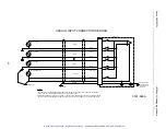
Страница 21: ...SHIELDED CABLE IS RECOMMENDED FOR LOWEST NOISE SHIELD IS CONNECTED TO GROUND REFERENCE AT ONE END ONLY TO PROVIDE SHIELDING WITHOUT GROUND LOOPS NOTES CH16 31 EXT SOURCE 16 31 SEE NOTE 2 SEE NOTE 1 SH...

Страница 22: ...uipment Have surplus equipment taking up shelf space We ll give it a new home Learn more Visit us at artisantg com for more info on price quotes drivers technical specifications manuals and documentat...

Отзывы: