background image


ORDER NO.


PIONEER CORPORATION   

4-1, Meguro 1-chome, Meguro-ku, Tokyo 153-8654, Japan

PIONEER ELECTRONICS (USA) INC.  P.O. Box 1760, Long Beach, CA 90801-1760, U.S.A.
PIONEER EUROPE NV  Haven 1087, Keetberglaan 1, 9120 Melsele, Belgium
PIONEER ELECTRONICS ASIACENTRE PTE. LTD.  253 Alexandra Road, #04-01, Singapore 159936

    PIONEER CORPORATION 2004


DEH-P670MP/XN/UC


CRT3335


MULTI-CD CONTROL HIGH POWER CD/MP3/WMA PLAYER WITH FM/AM TUNER


DEH-P670MP


/XN/UC


DEH-P6700MP


/XN/UC


DEH-P6750MP


/XN/ES


This service manual should be used together with the following manual(s):


Model No.

Order No.

Mech.Module

Remarks


CX-3158

CRT3394

S10.1AAC

CD Mech. Module:Circuit Description, Mech. Description, Disassembly

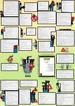
For details, refer to "Important Check Points for Good Servicing". 


K-ZZU.DEC.  2004 Printed in Japan

Summary of Contents for DEH-P6750MP

Page 1: ...01 Singapore 159936 PIONEER CORPORATION 2004 DEH P670MP XN UC CRT3335 MULTI CD CONTROL HIGH POWER CD MP3 WMA PLAYER WITH FM AM TUNER DEH P670MP XN UC DEH P6700MP XN UC DEH P6750MP XN ES This service manual should be used together with the following manual s Model No Order No Mech Module Remarks CX 3158 CRT3394 S10 1AAC CD Mech Module Circuit Description Mech Description Disassembly For details ref...

Page 2: ...s lead in solder and certain electrical parts contain chemicals which are known to the of California to cause cancer birth defects or other reproductive harm Health Safety Code Section 25249 6 Proposition 65 repair warranty trying to do so state Service Precaution 1 You should conform to the regulations governing the product safety radio and noise and other regulations and should keep the safety d...

Page 3: ...ide the product Please check that neither solder debris nor screws remain inside the product 8 There should be no semi broken wires scratches melting etc on the coating of the power cord Damaged power cords may lead to fire accidents so please be sure that there are no damages If you find a damaged power cord please exchange it with a suitable one 9 There should be no spark traces or similar marks...

Page 4: ...NIT 24 3 4 CD MECHANISM MODULE GUIDE PAGE 26 4 PCB CONNECTION DIAGRAM 36 4 1 TUNER AMP UNIT 36 4 2 PANEL UNIT 40 4 3 KEYBOARD UNIT 42 4 4 CD CORE UNIT S10 1 44 5 ELECTRICAL PARTS LIST 46 6 ADJUSTMENT 52 6 1 OEL UNIT ADJUSTMENT 52 6 2 CD ADJUSTMENT 53 6 3 CHECKING THE GRATING AFTER CHANGING THE PICKUP UNIT 55 6 4 ERROR MODE 57 6 5 DOT CLOCK ADJUSTMENT 58 7 GENERAL INFORMATION 59 7 1 DIAGNOSIS 59 7 ...

Page 5: ...DEH P670MP XN UC 5 5 6 7 8 5 6 7 8 C D F A B E 1 SPECIFICATIONS ...

Page 6: ...DEH P670MP XN UC 6 1 2 3 4 1 2 3 4 C D F A B E ...

Page 7: ...DEH P670MP XN UC 7 5 6 7 8 5 6 7 8 C D F A B E ...

Page 8: ...st The mark found on some component parts indicatesthe importance of the safety factor of the part Therefore when replacing be sure to use parts of identical designation Screw adjacent to mark on the product are used for disassembly For the applying amount of lobricants or glue follow the instructions in this manual In the case of no amount instructions apply as you think it appropriate ...

Page 9: ...der CND1250 CND1250 Not used 15 Bush CNV3930 CNV3930 CNV3930 16 Remote Control Unit CXC3173 CXC3173 CXC3173 17 Battery CEX1065 CEX1065 CEX1065 18 Carton XHG7079 XHG7078 XHG7076 19 Contain Box XHL7079 XHL7078 XHL7076 20 Protector XHP7003 XHP7003 XHP7003 21 Protector XHP7004 XHP7004 XHP7004 22 1 Owner s Manual XRD7074 XRD7065 XRD7067 22 2 Owner s Manual Not used Not used XRD7068 22 3 Installation Ma...

Page 10: ... 6 27 19 85 29 84 86 20 31 34 33 32 93 22 30 83 83 83 39 62 63 64 90 70 69 67 68 80 81 73 82 79 75 76 77 71 67 72 66 89 92 5 40 43 55 56 15 53 51 94 42 57 58 52 45 46 44 48 59 54 38 35 37 60 1 1 12 11 50 49 7 4 4 4 13 95 88 88 41 3 2 2 2 41 47 10 14 43 9 8 65 78 74 62 75 91 61 36 16 17 87 B C A ...

Page 11: ... 10A CEK1208 45 Pin Jack CN352 CKB1051 46 Plug CN901 CKM1376 47 Plug CN351 See Contrast table 2 48 Connector CN101 CKS3408 49 Plug CN801 CKS3537 50 Connector CN651 CKS3837 51 Connector CN161 See Contrast table 2 52 Antenna Jack CN401 CKX1056 53 Holder See Contrast table 2 54 Holder CND1352 55 Heat Sink CNR1668 56 Screw See Contrast table 2 57 FM AM Tuner Unit CWE1646 58 Holder CND1054 59 Insulator...

Page 12: ...0MP XN ES 5 Cord Assy CDE7129 Not used Not used 15 Holder Not used CNV7619 Not used 39 Panel XNS7088 XNS7089 XNS7088 40 Tuner Amp Unit XWM7096 XWM7097 XWM7098 47 Plug CN351 CKS1238 Not used Not used 51 Connector CN161 CKS4124 CKS4124 Not used 53 Holder CND1270 XNC7003 CND1477 56 Screw Not used BMZ40P140FTC Not used 61 Detachable Assy XXA7349 XXA7348 XXA7346 68 Button XAC7070 XAC7076 XAC7070 90 Sub...

Page 13: ...DEH P670MP XN UC 13 5 6 7 8 5 6 7 8 C D F A B E ...

Page 14: ...38 23 59 87 86 5 13 34 5 5 13 44 5 C 52 53 36 4 73 29 51 18 64 76 50 10 72 75 49 77 67 27 78 60 90 48 8 17 46 6 60 11 89 43 70 14 31 65 85 66 85 31 35 14 74 85 1 2 3 R 91 12 33 61 63 21 79 57 58 62 80 13 4 86 I 45 28 7 24 47 P 41 20 40 69 39 30 P 19 56 F E 22 81 15 G 26 5 54 37 55 93 92 10 D 1GEM1024 2GEM1045 3GEM1035 1 1 1 1 1 1 1 1 2 2 2 2 1 1 1 1 1 2 2 1 3 ...

Page 15: ...CNC9968 39 Arm CND1909 40 Lever CND2032 41 Lever CNC9984 42 Sheet CNM8134 43 Collar CNV7798 44 Guide CNV7799 45 Arm CNV8403 46 Rack CNV8374 47 Holder CNV8376 48 Holder CNV8377 49 Arm CNV8378 50 Gear CNV8379 51 Gear CNV8380 52 Gear CNV8381 53 Gear CNV8382 54 Gear CNV8383 55 Gear CNV8384 56 Rack CNV8385 57 Arm CNV8386 58 Arm CNV8387 59 Guide CNV8388 60 Roller CNV7218 61 Gear CNV8389 62 Arm CNV8391 6...

Page 16: ... T51 CF52 CF51 RFGND OSCGND DGND AUDIOGND NC VCC VDD_3 3 3 3V 2 5V IC 4 3 3V 2 5V IC 2 2 5V WC CE2 ROM_VDD SL DI CK CE1 NC DO NC NC NC NC 7 6 13 5 10 9 8 11 14 18 19 20 21 1 3 2 12 15 22 16 4 17 IC 1 3 3V AM ANT FMRF ATT LPF OSC IC 3 EEPROM 5 0V IC 5 5V 3 3V ATT MIXER IF AMP DET FM MPX 24 23 Rch Lch 91 CSENS ILB CONTROL BRST BRXEN BSRQ D CN901 Q101 M LASER DIODE MONITOR DIODE S903 DSCSNS FOCUS ACT...

Page 17: ... INDICATOR B UP 0 B UP Q852 6 7 2 13 13 9 12 12 7 ROT1 ROT0 VDD S 80835CNUA B8U 20 EMUTE 57 MUTE CN801 8 8 S1970 EJECT 9 9 DGND 5 6 5 6 0 RL Q351 2 CN351 RL REAR L OEL B VOLUME ENCORDER RL RL B UP GND ACC B REM ILM TEL FL FL B UP SL Q808 Q807 Q805 IC851 NJM2360M 1 OEL B DC DC CONVERTER SYS 8 3V B UP 1 2 NJM2388F84 4 IC910 SYS 8 3V REGULATOR Q982 PEG057A ISENS 81 Q932 Q913 Q981 Q803 Q804 ILM TEL P6...

Page 18: ...ms their resistance values or capacitance values are expressed in codes Ex Resistors Code Practical value 123 12k ohms 103 10k ohms Capacitors Code Practical value 103 0 01uF 101 10 100uF 10V The mark found on some component parts indicates the importance of the safety factor of the part Therefore when replacing be sure to use parts of identical designation Symbol indicates a resistor No different...

Page 19: ...ETACH SENSE 3A 3A CD 9 66dBs CD 10 01dBs REAR R ch REAR L ch SUB WOOFER R ch SUB WOOFER L ch FRONT R ch FRONT L ch BACK UP 10A FUSE CEK1208 IP BUS 9 30dBs CD 10 46dBs FM 5 80dBs AM 4 90dBs IP BUS 36 46dBs CD 35 30dBs FM 31 60dBs AM 21 10dBs A TUNER AMP UNIT ...

Page 20: ...DEH P670MP XN UC 20 1 2 3 4 1 2 3 4 C D F A B E A a A b A a A a A b 1 FM AM TUNER UNIT FM 19 5dBs AM 30 0dBs IP BUS 9 30 CD 10 46dBs FM 5 80dBs AM 4 90dBs IPBUS 2 2dBs ...

Page 21: ... 10k ohms Capacitors Code Practical value 103 0 01uF 101 10 100uF 10V The mark found on some component parts indicates the importance of the safety factor of the part Therefore when replacing be sure to use parts of identical designation Symbol indicates a resistor No differentiation is made between chip resistors and discrete resistors NOTE Symbol indicates a capacitor No differentiation is made ...

Page 22: ... 1 2 3 4 C D F A B E A a A b A b 1 3A 3A CD 9 66dBs CD 10 01dBs REAR R ch REAR L ch SUB WOOFER R ch SUB WOOFER L ch FRONT R ch FRONT L ch BACK UP 10A FUSE CEK1208 IP BUS 9 30dBs CD 10 46dBs FM 5 80dBs AM 4 90dBs A TUNER AMP UNIT ...

Page 23: ...DEH P670MP XN UC 23 5 6 7 8 5 6 7 8 C D F A B E A a A b A b 2 3 BACK UP 10A FUSE CEK1208 DETACH SENSE IP BUS 36 46dBs CD 35 30dBs FM 31 60dBs AM 21 10dBs ...

Page 24: ...DEH P670MP XN UC 24 1 2 3 4 1 2 3 4 C D F A B E 3 3 KEYBOARD UNIT C B CN1951 VOLUME ...

Page 25: ...DEH P670MP XN UC 25 5 6 7 8 5 6 7 8 C D F A B E C C KEYBOARD UNIT P670MP PD8142A P6700MP PD8141A P6750MP PD8141A 15k B 15k B OEL UNIT MXS8221 OEL CONTROLLER ...

Page 26: ...3 4 C D F A B E 3 4 CD MECHANISM MODULE GUIDE PAGE D a D TY PICKUP UNIT P10 SERVICE M1 CXC4440 SPINDLE MOTOR M2 CXB8933 LOADING CARRIAGE MOTOR CD DRIVER T F F T T T F F F T C S T F S C F F T T S S C C C C S S T T F F 1 3 2 0 9 7 8 5 4 ...

Page 27: ...IT S10 1 S901 HOME SWITCH ON OFF S903 DSCSNS SWITCH ON OFF S904 12EJ SWITCH ON OFF S905 8EJ SWITCH ON OFF The underlined indicates the switch position CD CORE UNIT S10 1 D A CN651 F SIGNAL LINE FOCUS SERVO LINE TRACKING SERVO LINE CARRIAGE SERVO LINE SPINDLE SERVO LINE T C S 3V REGULATOR 3 3V REGULATOR MICRO COMPUTER 6 ...

Page 28: ...DEH P670MP XN UC 28 1 2 3 4 1 2 3 4 C D F A B E D b D a D a D b 1 2 PICKUP UNIT P10 SERVICE T F F T T T F F F T C S T T F F ...

Page 29: ...DEH P670MP XN UC 29 5 6 7 8 5 6 7 8 C D F A B E D b D a D a D b 2 3 4 5 6 M1 CXC4440 SPINDLE MOTOR M2 CXB8933 LOADING CARRIAGE MOTOR CD DRIVER T F S C F F T T S S C C C C S S 1 3 2 0 9 7 8 5 4 ...

Page 30: ... UNIT S10 1 S901 HOME SWITCH ON OFF S903 DSCSNS SWITCH ON OFF S904 12EJ SWITCH ON OFF S905 8EJ SWITCH ON OFF The underlined indicates the switch position CD CORE UNIT S10 1 D F SIGNAL LINE FOCUS SERVO LINE TRACKING SERVO LINE CARRIAGE SERVO LINE SPINDLE SERVO LINE T C S 3 3V REGULATOR ...

Page 31: ...DEH P670MP XN UC 31 5 6 7 8 5 6 7 8 C D F A B E D a D b D b 2 3 4 5 6 SRAMLEVEL0 SRAMLEVEL1 SRAMLEVEL2 TYPE_A D A CN651 3V REGULATOR MICRO COMPUTER 6 ...

Page 32: ...00mV div 500mV div 500mV div 20ms div Ref REFO Mode Normal TE FE 500mV div 500mV div 200ms div Source On setup operation CD DA Play operation Ref REFO Mode Normal FE 0 FIN TE 9 TIN 500mV div 500mV div 500mV div 500mV div 20ms div CD ROM play operation Regular track Jump Ref REFO Mode Normal MDX 7 SIN 2V div 1V div 5µs div Ref REFO Mode Normal MDX 7 SIN 1V div 200mV div 50ms div Spindle waveform du...

Page 33: ... TIN 1V div 500mV div 500mV div 500ms div Ref REFO Mode Normal 1 DSCSNS 2 8SNS 3 12SNS 4 LOEJ 5V div 5V div 5V div 5V div 500ms div 12 cm CD Eject operation CD DA CD ROM mode change Band key Ref GND Mode Normal RFAGC TE 9 TIN 1V div 500mV div 500mV div 500µs div 4 Tracks Jump waveform 32 Tracks Jump waveform Ref REFO Mode TEST RFAGC TE 9 TIN 1V div 500mV div 500mV div 2ms div Ref REFO Mode TEST RF...

Page 34: ...3 4 C D F A B E 7 SIN 8 CIN 9 TIN 1V div 500mV div 500mV div 500ms div CD ROM CD DA mode change Band key Ref REFO Mode Normal RFAGC 9 TIN TE 0 FIN 1V div 1V div 1V div 1V div 500µs div Black dot 800µm during play Ref REFO Mode Normal ...

Page 35: ...DEH P670MP XN UC 35 5 6 7 8 5 6 7 8 C D F A B E ...

Page 36: ... A A TUNER AMP UNIT SIDE B SIDE A NOTE FOR PCB DIAGRAMS 1 The parts mounted on this PCB include all necessary parts for several destination For further information for respective destinations be sure to check with the schematic dia gram 2 Viewpoint of PCB diagrams D CN901 IP BUS WIRED REMOTE CONTROL CORD ASSY CORD ASSY DETACH SENSE ...

Page 37: ...DEH P670MP XN UC 37 5 6 7 8 5 6 7 8 C D F A B E A SIDE A B CN1950 FRONT SSY RCA ANTENNA FM AM TUNER UNIT ...

Page 38: ...DEH P670MP XN UC 38 1 2 3 4 1 2 3 4 C D F A B E A A TUNER AMP UNIT ...

Page 39: ...DEH P670MP XN UC 39 5 6 7 8 5 6 7 8 C D F A B E A SIDE B ...

Page 40: ...DEH P670MP XN UC 40 1 2 3 4 1 2 3 4 C D F A B E 4 2 PANEL UNIT B B PANEL UNIT B PANEL UNIT SIDE A SIDE B C CN1901 A CN801 EJECT ...

Page 41: ...DEH P670MP XN UC 41 5 6 7 8 5 6 7 8 C D F A B E ...

Page 42: ...DEH P670MP XN UC 42 1 2 3 4 1 2 3 4 C D F A B E 4 3 KEYBOARD UNIT C C KEYBOARD UNIT SIDE A CLK 6 5 4 3 2 1 SW OPEN E AUDIO FUNC EQ BAND VOL SRC DISP PAUSE OEL UNIT ...

Page 43: ...DEH P670MP XN UC 43 5 6 7 8 5 6 7 8 C D F A B E C C KEYBOARD UNIT SIDE B B CN1951 OEL UNIT TP1 TP2 TP3 ...

Page 44: ...DEH P670MP XN UC 44 1 2 3 4 1 2 3 4 C D F A B E 4 4 CD CORE UNIT S10 1 D D CD CORE UNIT S10 1 SIDE A A CN651 PICKUP UNIT P10 SERVICE HOME M2 LOADING CARRIAGE MOTOR M1 SPINDLE MOTOR E F REFO1 ...

Page 45: ...DEH P670MP XN UC 45 5 6 7 8 5 6 7 8 C D F A B E D D CD CORE UNIT S10 1 SIDE B 12EJ 8EJ DSCSNS ...

Page 46: ...istor 2SD2396 Q 913 B 30 69 Transistor UMD2N Q 931 A 61 78 Transistor UMX1N Q 932 B 78 86 Transistor DTC114EU Q 951 A 95 74 Transistor 2SA1576 Q 981 B 29 84 Transistor 2SC4081 Q 982 A 44 70 Transistor UMD2N D 131 A 118 113 Diode Network DA204U D 132 A 132 62 Diode Network DA204U D 133 A 138 60 Diode DAN202U D 301 A 68 113 Diode S5688G D 302 A 64 116 Diode S5688G D 303 A 88 98 Diode S5688G D 304 A ...

Page 47: ... R 416 B 97 57 RS1 16S681J R 417 B 113 50 RS1 16S681J R 419 B 125 53 RS1 16S681J R 421 B 125 51 RS1 16S681J R 601 B 108 59 P670MP P6750MP RS1 16S104J Circuit Symbol and No Part No R 602 B 101 56 P6700MP RS1 16S104J R 603 B 114 60 P670MP P6700MP RS1 16S104J R 604 B 114 57 P6750MP RS1 16S104J R 606 B 101 58 RS1 16S104J R 607 B 57 54 RS1 16S822J R 608 A 85 28 RS1 16S221J R 609 B 83 24 RS1 16S221J R 6...

Page 48: ... A 135 80 CEJQ4R7M35 C 217 A 114 73 CEJQ4R7M35 Circuit Symbol and No Part No C 218 A 136 73 CEJQ4R7M35 C 219 B 116 84 CCSRCH120J50 C 220 B 130 83 CCSRCH120J50 C 221 A 115 78 CCSRCH120J50 C 222 B 127 83 CCSRCH120J50 C 225 A 129 75 CEJQ100M16 C 241 B 96 80 CKSRYB152K50 C 242 B 129 89 CKSRYB152K50 C 306 A 96 99 CEJQ330M10 C 307 A 49 121 3300µF 16V CCH1486 C 309 B 46 123 CKSRYB104K16 C 310 A 112 118 C...

Page 49: ...S 1903 A 38 75 Push Switch CSG1174 S 1904 A 18 36 Push Switch CSG1174 S 1905 A 7 8 Push Switch CSG1155 S 1906 A 36 15 Push Switch CSG1155 S 1907 A 38 91 Push Switch CSG1174 S 1908 A 38 67 Push Switch CSG1174 S 1909 A 38 52 Push Switch CSG1174 S 1910 A 38 37 Push Switch CSG1174 S 1911 A 38 129 Push Switch CSG1174 S 1912 A 38 114 Push Switch CSG1174 S 1913 A 38 99 Push Switch CSG1174 S 1914 A 11 137...

Page 50: ...1389 L 207 A 53 31 Inductor CTF1389 Circuit Symbol and No Part No L 209 A 26 20 Inductor CTF1389 L 703 A 64 49 Inductor CTF1389 X 201 A 51 35 Ceramic Resonator 16 934MHzCSS1603 X 701 A 59 53 Ceramic Resonator 4 00MHzCSS1652 S 901 A 15 43 Switch HOME CSN1067 S 903 B 53 100 Switch DSCSNS CSN1068 S 904 B 35 108 Switch 12EJ CSN1067 S 905 B 48 109 Switch 8EJ CSN1067 RESISTORS R 101 A 22 24 RS1 10SR2R4J...

Page 51: ... B 35 8 CCSSCH560J50 C 223 B 33 8 CCSSCH4R0C50 C 224 B 40 16 CKSSYB104K10 C 225 B 45 14 CKSSYB103K16 C 226 B 43 12 CCSSCH680J50 C 227 A 45 10 CCSSCH470J50 C 228 A 49 9 CKSSYB103K16 C 234 B 36 81 CEVW221M4 C 237 B 38 29 CKSSYB104K10 C 239 B 34 10 CCSSCH220J50 C 242 B 58 32 CKSSYB104K10 C 243 B 39 76 CKSSYB104K10 C 244 B 49 70 CKSSYB104K10 C 246 A 23 19 CKSSYB104K10 C 251 B 28 31 CKSRYB102K50 C 260 ...

Page 52: ...6 1 OEL UNIT ADJUSTMENT When the OEL Unit has been replaced 1 Use VR1970 to adjust the resistance between TP1 and TP3 to 6 2kΩ 2 Use VR1971 to adjust the resistance between TP2 and TP3 to 6 2kΩ Digital Multi Meter KEYBOARD UNIT SIDE B Adjustment point TP1 TP2 TP3 ...

Page 53: ...ections will not work Avoid applying any mechanical or electrical shock to the mechanism during adjustment The RFI and RFO signals with a wide frequency range are easy to oscillate When observing the signals insert a resistor of 1k ohms in series The load and eject operation is not guarantied with the mechanism upside down If the mechanism is blocked due to mistaken eject operation reset the produ...

Page 54: ... SEC8x or TRK9xMIN9xSEC9x TRKSPMINSPSECSP 4 TRKGGMINGGSECGG 2 Key BAND 6 1 2 3 Power On Off CRG TR Jump Direction of the external surface CRG TR Jump Direction of the internal surface U CLS and AGC and Applicable servomechanism AGC AGC display setting RF Gain switching Offset adjustment display T Balance adjustment T Open Close S Curve Rough Servo and RF AGC SPDL 1X 2X switching As for the double ...

Page 55: ...d switch the 3V regulator on 2 Using the and buttons move the PU unit to the innermost track 3 Press key 3 to close focus the display should read 91 Press key 2 to implement the tracking balance adjustment the display should now read 81 Press key 3 The display will change returning to 81 on the fourth press 4 As shown in the diagram above monitor the LPF outputs using the oscilloscope and check th...

Page 56: ...DEH P670MP XN UC 56 1 2 3 4 1 2 3 4 C D F A B E Grating waveform 45 0 75 60 30 90 Ech Xch 20mV div AC Fch Ych 20mV div AC ...

Page 57: ...3 or WMA file present in a disc No MP3 or WMA file exists in a CD ROM disc inserted 17 Electricity Setup NG AGC protection doesn t work out of Focus soon Scratch on Disc Severe dirt and vibration 12 Electricity Spindle Lock NG Not spindle lock Wrong subcode can t read Subcode NG RF amp NG Defective Spindle Scratch and dirt on Disc Intense vibration The appropriate gain of the RF amp cannot be obta...

Page 58: ...e ACC switched ON the standby mode cancelled shift the TESTIN Pin 86 terminal to H The clock signal is output from the PCL terminal Pin 37 The frequency of the clock signal is 312 5kHz that is one 32th of the fundamental frequency The clock signal should be 312 5kHz If the clock signal is out of the range the X tal X601 should be replaced with new one ...

Page 59: ...1 1 Fig 2 Tuner Amp Unit Removing the Tuner Amp Unit Fig 2 Remove the screw 1 Remove the four screws Disconnect the connector and then remove the CD Mechanism Module 2 Remove the two screws and then remove the Grille Assy 2 2 1 2 2 2 3 3 3 4 Remove the three screws 2 Straighten the tabs at three locations indicated 3 Remove the screw and then remove the Tuner Amp Unit 4 The Tuner Amp Unit may appe...

Page 60: ...he two springs C and the four screws 2 To remove the upper frame open it on the fulcrum A 3 While lifting the carriage mechanism remove the three dampers 4 With the frames removed insert the connectors coming from the main unit and eject the disc Caution Before installing the carriage mechanism in the frames be sure to apply some alcohol to the dampers and set the mechanism to the clamp mode Do no...

Page 61: ...ead wires from the inner holder 4 Remove the washer styling holder change arm and pickup lock arm 5 While releasing from the hook of the inner holder lift the end of the feed screw Caution In assembling move the planet gear to the load eject position before setting the feed screw in the inner holder Shorting Solder Planet Gear Change Arm Inner Holder Styling Holder Feed Screw Washer Pickup Lock Ar...

Page 62: ... 1 BUS 2 GND 3 GND 4 NC 5 BUS 6 GND 7 BUS L INPUT 8 ASENB 9 BUS R INPUT 10 BUS R INPUT 11 BUS L INPUT IP BUS WIRED REMOTE CONTROL P670MP P6700MP REAR OUTPUT P670MP 11 10 9 8 7 6 5 4 3 2 1 9 RL 10 FL 11 RL 12 FL 13 RR 14 FR 15 RR 16 FR 1 BACK UP 2 GND 3 ACC 4 NC 5 ILM 6 B REM 7 NC 8 TEL MUTE POWER SUPPLY SPEAKER OUTPUT 15 1 13 11 9 7 5 3 16 2 14 12 10 8 6 4 ...

Page 63: ...DEH P670MP XN UC 63 5 6 7 8 5 6 7 8 C D F A B E 7 2 IC NJM2388F84 IN 1 GND 2 OUT 3 Bandgap Reference Thermal Protection NJM2885DL1 33 ...

Page 64: ... 27 BRXEN I O C It is possible to receive P Bus 28 bsrq I O C P Bus service request demand 29 NC Not used 30 DSCSNS I Disc state sense input 31 8EJ S905 I Input of detection of 8 cm disc ejection 32 12EJ S904 I Input of detection of 12 cm disc ejection 33 EVSS E power supply GND 34 EVDD E power supply Positive power supply 35 36 SRAMLEVEL0 1 O C SRAM level meter output 37 EMPH O C Emphasis informa...

Page 65: ...ogram starting input 97 HOME I Home SW sense input 98 TEMP I Temperature information sense input 99 VDSENS I VD power supply short sense input 100 NC Not used PE5454A 25 26 50 51 75 76 100 1 Format Meaning C CMOS IC s marked by are MOS type Be careful in handling them because they are very liable to be damaged by electrostatic induction 2 10 11 12 13 14 15 16 17 18 19 20 21 22 35 34 33 32 31 30 29...

Page 66: ...I P BUS Serial data input 31 BSCK O P BUS Serial clock output 32 CDCONT O S10 CD power supply control output 33 DPDT O GRILLE Data output 34 KYDT I GRILLE Data input 35 36 ROT1 0 I Rotary encoder pulse input1 0 37 PCL O Output for clock adjustment 38 SWVDD O GRILLE Chip enable output 39 dsens I Detach sense input 40 FLPILM O Illumination output inside flap 41 ILMPW O Illumination output 42 ejtin I...

Page 67: ...sc position detection input 88 VDSENS I S10 VD power supply short sense input 89 KEYAD I Key data input 90 LVLINR I Level indicator Rch input 91 CSENS I Flap opening and closing sense input 92 LVLINL I Level indicator Lch input 93 ASLIN I ASL input 94 AVSS AD translation power supply input terminal 95 SL I TUNER Signal level input 96 VREF AD translation reference voltage 97 AVCC AD translation pow...

Page 68: ...ation 29 DA2 O C Display data MSB 30 NC Not used 31 CLK1 I UART1 clock input 32 ILMD O C Dual illumination 33 DA1 O C Display data LSB 34 NC Not used 35 CLK0 I UART0 clock input 36 NC O Not used OPEN 37 rdy I Not used Pull up 38 NC Not used OPEN 39 hold I Pull up 40 NC OPEN 41 cs r Not used Pull up 42 rd O C Read strobe 43 NC OPEN 44 wr O C Not used OPEN 45 cs O C Not used OPEN 46 cs O C Bank addr...

Page 69: ...670MP XN UC 69 5 6 7 8 5 6 7 8 C D F A B E PEG090A HA12240FP 25 26 50 51 75 76 100 1 Format Meaning C CMOS N Nch open drain 1 3 2 S1 R S2 GND BUS BUS VCC STB 4 5 6 7 8 BIAS DRIVER OUTPUT COM RECEIVER OUTPUT ...

Page 70: ... I Connected to GND 42 PWMSW1 I Setup 1 for PWM output FD TD 43 TESTEN I Connected to GND 44 D1 GND GND for 1 6V digital circuits 45 DIN I Input of audio data 46 DOUT O Output of audio data 47 SCKIN I Clock input for audio data 48 SCKO O Clock output for audio data 49 LRCKIN I Input of LRCK for audio data 50 LRCK O Output LRCK for audio data 51 xtalen I Permission to oscillate 16 9344MHz 52 D1 VDD...

Page 71: ...GCO O Output of RF 117 C3T O Connection to the capacitor for detecting 3T 118 AGCI I Input of AGC 119 RFO O Output of RF AGC 120 121 EQ2 1 I Equalizer 2 1 122 RF2 I Reversal input of RF2 123 RF I Reversal input of RF 124 A GND Ground for the analog system 125 A I Input of A 126 C I Input of C 127 B I Input of B 128 D I Input of D 129 F I Input of F 130 E I Input of E 131 VREFIN I Input of referenc...

Page 72: ...I I data in Data input 11 NC non connection Not used 12 OSCGND osc ground Ground of oscillator block 13 ROM_VDD power supply Power supply for EEPROM pin 13 is connected with a power supply of micro computer 14 DO O data out Data output 15 DGND digital ground Ground of digital block 16 NC non connection Not used 17 VDD_3 3 power supply The power supply for digital block 3 3V 0 2V 18 NC non connecti...

Page 73: ... on operation After that proceed to each source operation SYSPW H Pin 1 Starts communication with Grille microcomputer Source ON 300ms 300ms In case of the above signal the communication with Grille microcomputer may fail If the time interval is not 300msec the oscillator may be defective CSENS Pin 91 2V CSENS 3V CSENS 2V 3V CSENS Last source returns CD loading functions are available Keys except ...

Page 74: ...C D F A B E 7 4 CLEANING Before shipping out the product be sure to clean the following portions by using the prescribed cleaning tools Portions to be cleaned Cleaning tools CD pickup lenses Cleaning liquid GEM1004 Cleaning paper GED 008 ...

Page 75: ...DEH P670MP XN UC 75 5 6 7 8 5 6 7 8 C D F A B E 8 OPERATIONS ...

Page 76: ...DEH P670MP XN UC 76 1 2 3 4 1 2 3 4 C D F A B E ...

Page 77: ...DEH P670MP XN UC 77 5 6 7 8 5 6 7 8 C D F A B E ...

Page 78: ...DEH P670MP XN UC 78 1 2 3 4 1 2 3 4 C D F A B E ...

Page 79: ...DEH P670MP XN UC 79 5 6 7 8 5 6 7 8 C D F A B E ...

Page 80: ...DEH P670MP XN UC 80 1 2 3 4 1 2 3 4 C D F A B E ...

Page 81: ...DEH P670MP XN UC 81 5 6 7 8 5 6 7 8 C D F A B E ...

Page 82: ...ews and holders to fix the front panel to this unit 1 Attach the holders to both sides of the front panel 2 Replace the front panel to the unit 3 Flip the holders into upright positions 4 Fix the front panel to the unit using fixing screws Fixing Screw BPZ20P060FZK UC model CXX1646 ES model Holder CND1249 UC model CXX1644 ES model Holder CND1250 UC model CXX1645 ES model ...

Page 83: ...on Red To electric terminal controlled by ignition switch 12 V DC ON OFF Orange white To lighting switch terminal Black ground To vehicle metal body Blue white To system control terminal of the power amp or Auto antenna relay control terminal max 300 mA 12 V DC Front speaker Front speaker With a 2 speaker system do not connect anything to the speaker leads that are not connected to speakers Rear s...

Page 84: ...DEH P670MP XN UC 84 1 2 3 4 1 2 3 4 C D F A B E Jigs List Test Disc L P F TCD 784 Checking the grating g g g Checking the grating g g g Two pieces Name Jig No Remarks ...

Reviews: