background image

SERVICE MANUAL

DVD PLAYER

EWD7003

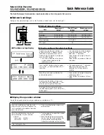
This service manual is for the EWD7003 Updated 
Version that the serial number is later than D39310001.
The model differs from the previous EWD7003, and that a 
star mark ( 

 ) is printed on the rating label is its 

applicable model. For the rating label on the rear panel, 
refer to below.

star mark

serial number

rating label

Summary of Contents for EWD7003

Page 1: ... Updated Version that the serial number is later than D39310001 The model differs from the previous EWD7003 and that a star mark is printed on the rating label is its applicable model For the rating label on the rear panel refer to below star mark serial number rating label ...

Page 2: ...ssible hazardous consequences of each way Consequently Funai has not undertaken any such broad evaluation Accordingly a servicer who uses a service procedure or tool which is not recommended by Funai must first use all precautions thoroughly so that neither his safety nor the safe operation of the equipment will be jeopardized by the service method selected TABLE OF CONTENTS SPECIFICATIONS 1 1 1 L...

Page 3: ...mp 100 K ohm 4 Room ambient 5 C 40 C ITEM CONDITIONS UNIT NOMINAL LIMIT 1 Video Output 75 ohm load Vpp 1 0 0 1 2 Coaxial Digital Out 75 ohm load mVpp 500 100 3 Audio PCM 3 1 Output Level 1kHz 0dB Vrms 2 0 3 2 S N dB 120 3 3 Freq Response DVD fs 48kHz 20 22kHz dB 0 5 CD fs 44 1kHz 20 20 kHz dB 0 5 3 4 THD N DVD 1 kHz 0dB 0 0025 CD 1 kHz 0dB 0 003 ...

Page 4: ...tion shown in the figure When checking the laser diode be sure to keep your eyes at least 30cm away from the pickup lens when the diode is turned on Do not look directly at the laser beam Caution Use of controls and adjustments or doing procedures other than those specified herein may result in hazardous radiation exposure Do not look directly at the laser beam coming from the pickup or allow it t...

Page 5: ...especially 1 Wires covered with PVC tubing 2 Double insulated wires 3 High voltage leads D Use specified insulating materials for hazardous live parts Note especially 1 Insulation tape 2 PVC tubing 3 Spacers 4 Insulators for transistors E When replacing AC primary side components transformers power cord etc wrap ends of wires securely about the terminals before solder ing F Observe that the wires ...

Page 6: ...ference only Be sure to confirm the precise values 2 Leakage Current Test Confirm the specified or lower leakage current between B earth ground power cord plug prongs and externally exposed accessible parts RF termi nals antenna terminals video and audio input and output terminals microphone jacks earphone jacks etc is lower than or equal to the specified value in the table below Measuring Method ...

Page 7: ...ve the flat pack IC with tweezers while apply ing the hot air 3 Bottom of the flat pack IC is fixed with glue to the CBA when removing entire flat pack IC first apply soldering iron to center of the flat pack IC and heat up Then remove glue will be melted Fig S 1 6 4 Release the flat pack IC from the CBA using twee zers Fig S 1 6 Caution 1 Do not supply hot air to the chip parts around the flat pa...

Page 8: ...l pins of the flat pack IC you can remove it easily Fig S 1 3 2 Affix the wire to a workbench or solid mounting point as shown in Fig S 1 5 3 While heating the pins using a fine tip soldering iron or hot air blower pull up the wire as the solder melts so as to lift the IC leads from the CBA contact pads as shown in Fig S 1 5 4 Bottom of the flat pack IC is fixed with glue to the CBA when removing ...

Page 9: ...ur due to a potential difference caused by electro static charge during unpacking or repair work 1 Ground for Human Body Be sure to wear a grounding band 1MΩ that is prop erly grounded to remove any static electricity that may be charged on the body 2 Ground for Workbench 1 Be sure to place a conductive sheet or copper plate with proper grounding 1MΩ on the workbench or other surface where the sem...

Page 10: ...nent video in jacks 16 S VIDEO OUT connect to a TV with S Video inputs Caution Do not touch the inner pins of the jacks on the rear panel Electrostatic discharge may cause permanent damage to the player 9 PAUSE pause playback temporarily frame by frame playback 10 REVh h to view DVD picture in fast reverse motion 11 PLAY to start a DVD disc playback 12 SETUP to access or remove the DVD setup menu ...

Page 11: ...ase two Locking Tabs A at the side and then three Locking Tabs B at the bottom 1 7 Release three Locking Tabs L 4 Then remove the Front Assembly CAUTION 2 Electrostatic breakdown of the laser diode in the optical system block may occur as a potential difference caused by electrostatic charge accumulated on cloth human body etc during unpacking or repair work To avoid damage of pickup follow next p...

Page 12: ...embly Tray Panel A A L 3 L 1 L 1 B L 2 L 4 L 4 3 DVD Mecha S 2 S 2 CN201 CN301 Fig D3 View for B Pickup Unit C B Short the three short lands by soldering Short the three short lands by soldering FPC Cable Connector Slide DVD Mecha View for C View for A OR A Fig D4 ...

Page 13: ...N601 CN2001 CN401 S 4 6 Function CBA Fig D5 S 7 8 Rear Panel S 6 7 Main CBA Holder Fig D6 Rotate this roulette in the direction of the arrow A View for A HOW TO MANUAL EJECT 1 Remove the Top Case 2 Rotate the roulette in the direction of the arrow as shown below ...

Page 14: ...OR IC101 MICRO CONTROLLER SLED MOTOR DRIVE FOCUS ACTUATOR DRIVE SPINDLE MOTOR DRIVE TRACKING ACTUATOR DRIVE 147 TRAY OUT TRAY IN FG IN 66 SLD 75 SPDL 76 TRACKING DRIVE 148 FOCUS DRIVE 69 72 TO DIGITAL SIGNAL PROCESS BLOCK DIAGRAM FS FS TS TS TO VIDEO AUDIO BLOCK DIAGRAM 57 ADAC MD 56 ADAC MC 58 ADAC ML ADAC MC ADAC ML PCM SCLK 55 A MUTE ADAC MD A MUTE 163 PCM SCLK RESET 73 RESET IC461 5 4 3 3V TRA...

Page 15: ...ATA RAM DSP DECODER I O PROCESSOR INST ROM DATA RAM INST ROM SERIAL D A GENERAL I O INTERRUPT CONTROLLER TIMER WATCH DOG TIMER REMOTE CONTROL 32BIT CPU STREAM I F EXTERNAL MEMORY I F SDRAM ECC UMAC 115 114 117 116 132 131 134 133 129 130 126 124 125 123 83 DEBUG BCU INST RAM DATA RAM D A D A D A TO VIDEO AUDIO BLOCK DIAGRAM 149 158 Y C Cr Cb VIDEO Y VIDEO C VIDEO Cr VIDEO Cb TO VIDEO AUDIO BLOCK D...

Page 16: ...AC LPF AMP L CH R CH LPF AMP DAC ZERO DETECT SYSTEM CLOCK 1 2 6 7 5 AUDIO R OUT PCM BCK SPDIF PCM DATA PCM LRCLK ADAC MD ADAC MC ADAC ML PCM SCLK AV CBA DVD MAIN CBA UNIT AUDIO SIGNAL DATA AUDIO SIGNAL 16 16 SPDIF A MUTE 3 3V Q1204 3 CN601 5 5 VIDEO Y 7 7 VIDEO C 3 3 VIDEO Cb 1 1 VIDEO Cr VIDEO Y VIDEO C VIDEO Cb VIDEO Cr JK1401 S VIDEO OUT CN1601 3 4 2 1 IC1402 VIDEO DRIVER 18 4dB AMP 2dB AMP LPF...

Page 17: ... 1 2 3 EV 1 2V 4 5 EV 3 3V 8 9 EV 11V 7 P ON 5V 6 P ON 3 3V 19 PWRCON 1 2V REG IC1002 REPLACE FUSE AS MARKED Ce symbole reprèsente un fusible à fusion rapide CAUTION FOR CONTINUED PROTECTION AGAINST FIRE HAZARD REPLACE ONLY WITH THE SAME TYPE FUSE ATTENTION POUR UNE PROTECTION CONTINUE LES RISQES D INCELE N UTILISER QUE DES FUSIBLE DE MÊME TYPE RISK OF FIRE This symbol means fast operating fuse A ...

Page 18: ... in the schematic diagram and the parts list Before replacing any of these components read the parts list in this manual carefully The use of substitute replacement parts that do not have the same safety characteristics as speci fied in the parts list may create shock fire or other hazards Notes 1 Do not use the part number shown on these draw ings for ordering The correct part number is shown in ...

Page 19: ...iability of repaired units use only original replacement parts which are listed with their part numbers in the parts list section of the service manual 4 Wire Connectors 1 Prefix symbol CN means connector can disconnect and reconnect 2 Prefix symbol CL means wire solder holes of the PCB wire is soldered directly 5 Voltage indications for PLAY and STOP mode on the schematics are as shown below 6 Ho...

Page 20: ...DATA VIDEO AUDIO TRACKING SERVO SIGNAL SPINDLE SERVO SIGNAL SLED SERVO SIGNAL DVD Main 1 3 Schematic Diagram 1 8 3 1 8 4 E58T0SCD1 DVD MAIN 1 3 Ref No Position IC201 B 1 IC202 D 4 IC301 D 3 IC461 E 1 Q251 C 2 Q252 B 2 Q253 C 2 Q254 B 2 CN201 A 3 CN301 A 1 CN401 F 3 CONNECTORS ICS TRANSISTORS ...

Page 21: ...3 J4 K1 K2 K3 K4 L1 L2 L3 L4 FOCUS SERVO SIGNAL DATA VIDEO AUDIO TRACKING SERVO SIGNAL SPINDLE SERVO SIGNAL SLED SERVO SIGNAL VIDEO SIGNAL DATA AUDIO DVD Main 2 3 Schematic Diagram 1 8 5 1 8 6 E58T0SCD2 DVD MAIN 2 3 Ref No Position IC101 H 4 IC ...

Page 22: ... 0 4 0 4 62 3 4 3 4 94 126 0 2 0 2 31 0 9 0 6 63 0 0 95 127 2 3 2 3 32 64 0 0 96 128 1 7 1 7 PIN NO PLAY STOP PIN NO PLAY STOP PIN NO PLAY STOP PIN NO PLAY STOP 129 2 3 2 3 161 3 3 3 3 193 225 3 4 3 4 130 2 2 2 2 162 0 0 194 226 131 2 4 2 4 163 1 6 1 6 195 227 132 2 4 2 4 164 0 0 196 3 4 3 4 228 133 2 4 2 4 165 1 5 1 5 197 229 0 0 134 2 4 2 4 166 1 6 1 6 198 230 135 167 3 4 3 4 199 231 3 4 3 4 136...

Page 23: ...4 O1 O2 O3 O4 P1 P2 P3 P4 Q1 Q2 Q3 Q4 R1 R2 R3 R4 AUDIO SIGNAL DATA AUDIO VIDEO SIGNAL DVD Main 3 3 Schematic Diagram 1 8 9 1 8 10 E58T0SCD3 DVD MAIN 3 3 Ref No Position IC102 O 4 IC103 N 3 IC601 P 1 CN601 R 2 ICS CONNECTOR ...

Page 24: ...TION AGAINST FIRE HAZARD REPLACE ONLY WITH THE SAME TYPE FUSE ATTENTION POUR UNE PROTECTION CONTINUE LES RISQES D INCELE N UTILISER QUE DES FUSIBLE DE MÊME TYPE RISK OF FIRE REPLACE FUSE AS MARKED This symbol means fast operating fuse Ce symbole reprèsente un fusible à fusion rapide CAUTION Fixed voltage or Auto voltage selectable power supply circuit is used in this unit If Main Fuse F1001 is blo...

Page 25: ...1 K2 K3 K4 L1 L2 L3 L4 AUDIO SIGNAL DATA AUDIO VIDEO SIGNAL AV 2 3 Schematic Diagram 1 8 13 1 8 14 E58T0SCAV2 AV 2 3 Ref No Position IC1201 H 1 IC1402 I 3 Q1201 J 1 Q1202 J 1 Q1203 I 2 Q1204 I 1 Q1351 J 4 Q1352 H 2 CN1601 G 3 ICS TRANSISTORS CONNECTOR ...

Page 26: ...2 M3 M4 N1 N2 N3 N4 O1 O2 O3 O4 P1 P2 P3 P4 Q1 Q2 Q3 Q4 AV 3 3 Function Schematic Diagram 1 8 15 1 8 16 E58T0SCAV3 AV 3 3 Ref No Position IC2001 O 3 Q2001 O 3 Q2003 P 3 CN2001 P 2 IC CONNECTORS TRANSISTORS ...

Page 27: ...N UTILISER QUE DES FUSIBLE DE MÊME TYPE RISK OF FIRE REPLACE FUSE AS MARKED This symbol means fast operating fuse Ce symbole reprèsente un fusible à fusion rapide CAUTION Fixed voltage or Auto voltage selectable power supply circuit is used in this unit If Main Fuse F1001 is blown check to see that all components in the power supply circuit are not defective before you connect the AC plug to the A...

Page 28: ...l means fast operating fuse Ce symbole reprèsente un fusible à fusion rapide CAUTION Fixed voltage or Auto voltage selectable power supply circuit is used in this unit If Main Fuse F1001 is blown check to see that all components in the power supply circuit are not defective before you connect the AC plug to the AC power supply Otherwise it may cause some components in the power supply circuit to f...

Page 29: ...FUNCTION CBA Top View FUNCTION CBA Bottom View 1 8 21 BE5800F01011B 1 8 22 ...

Page 30: ...TOP MODE WF1 WF3 WAVEFORMS WF6 SPDIF Pin 16 of CN1601 1V 0 1µsec WF1 Pin 5 of CN1601 WF3 Pin 21 of IC1402 WF4 AUDIO L Pin 11 of CN1601 1V 0 5msec WF5 AUDIO R Pin 13 of CN1601 1V 0 5msec WF2 Pin 7 of CN1601 VIDEO Y 0 2V 20µsec VIDEO C 0 2V 20µsec VIDEO CVBS 0 5V 20µsec ...

Page 31: ...N1001 CN2001 CN2002 VIDEO Cr 1 1 GND 2 2 VIDEO Cb 3 3 A MUTE 10 10 GND 9 9 GND 4 4 VIDEO Y 5 5 GND 6 6 VIDEO C 7 7 GND 8 8 CN601 CN1601 AC CORD AUDIO L OUT AUDIO R OUT VIDEO OUT DIGITAL AUDIO OUT S VIDEO OUT EV 1 2V 3 3 K2 3 3 K1 4 4 KEY 2 5 5 KEY 3 6 6 KEY 1 7 7 KEY 4 8 8 DRIVE CBA 19 20 VIDEO Y OUT VIDEO Cb OUT VIDEO Cr OUT SPDIF 16 16 AUDIO L 11 11 A L MUTE 12 12 AUDIO R 13 13 A R MUTE 14 14 AU...

Page 32: ...Turn the power on by pressing the power button and the tray will close 8 Press 1 2 3 4 and DISPLAY buttons on the remote control unit in that order Fig d appears on the screen 9 Press 3 button on the remote control unit Fig e appears on the screen 10 To exit this mode press POWER button F W Version Up Mode Please insert a DISC for F W Version Up EXIT POWER Fig a Version Up Mode Screen 1 previous v...

Page 33: ...ray IN TL221 3 3V 0V 0V 3 3V 0V 1 65V 0V 0V 0V 1 65V 1 65V 1 65V Tray OUT TL220 Sled Drive TP303 Disc Drive TP301 Focus Drive TP304 Tracking Drive Tracking Drive TP302 Tray Close Disc Rotation Play Disc Stop Tray Open SYSTEM CONTROL TIMING CHARTS ...

Page 34: ...ource 1 8 Out KEY 2 Key Source 2 9 Out KEY 3 Key Source 3 10 Out KEY 4 Key Source 4 11 NU Not Used 12 NU Not Used 13 NU Not Used 14 NU Not Used 15 NU Not Used 16 NU Not Used 17 Out PLAY LED Play LED Display Signal 18 Out DISC IN LED Loading Disc LED Display Signal 19 NU Not Used 20 NU Not Used 21 NU Not Used 22 NU Not Used 23 NU Not Used 24 VDD Power Supply 25 VSS GND 26 In OSC Oscillator Input 27...

Page 35: ...120 Y TPE2 KTC3203 Y KRC101M BA1L3M T E C B 2SC2785 H KTC3199 GR KTA1267 Y A K C E LTV 817 B C F KIA431 AT FAN431AZXA 2SK3374 PQ070XF01SZ K A R 1 2 3 4 Note A Anode K Cathode E Emitter C Collector B Base R Reference G Gate D Drain S Source 1 Vin 2 Vo 3 GND 4 Vc 24 13 12 MM1622XJBE 1 S D G LEAD IDENTIFICATIONS ...

Page 36: ...al Parts List for parts with this mark Some Ref Numbers are not in sequence AV CBA 2B3 2L105 F1001 2L031 1B1 A19 2L021 A2 2L021 2L021 JK1202 JK1401 A21 A22 JK1404 A13 A23 A1X 2L011 2L011 2L011 A16 2L011 2L011 2L041 A13 2L101 FUNCTION CBA AC1001 EXPLODED VIEWS Cabinet ...

Page 37: ...1 15 2 E58T0EX X10 X5 X2 X4 S4 Unit S1 A22 X1 S2 S2 S5 X14 X36 Packing ...

Page 38: ...BER H7931UD EMER SON 1B1 DVD MECHA THIN TYPE 0838 VCDVM040 N79F1GVM 2B3 HOLDER MAIN PCB E5700UD 0VM305832B 2L011 SCREW C TIGHT M3X5 BIND HEAD GBCC3050 2L021 SCREW S TIGHT M3X8 BIND CHROME GBMS3080 2L031 SCREW C TIGHT M3X6 BIND HEAD GBMC3060 2L041 SCREW B TIGHT M3X8 BIND HEAD GBKB3080 2L071 SCREW C TIGHT M3X6 BIND HEAD GBMC3060 2L101 SCREW C TIGHT M3X6 BIND HEAD GBMC3060 2L105 P TIGHT SCREW 3X8 BIN...

Page 39: ...MASDL100 C1202 ELECTROLYTIC CAP 10µF 16V M CE1CMASDL100 C1205 CHIP CERAMIC CAP CH J 220pF 50V CHD1JJ3CH221 C1206 CHIP CERAMIC CAP CH J 220pF 50V CHD1JJ3CH221 C1207 CHIP CERAMIC CAP CH J 47pF 50V CHD1JJ3CH470 C1208 CHIP CERAMIC CAP CH J 47pF 50V CHD1JJ3CH470 C1221 ELECTROLYTIC CAP 10µF 16V M CE1CMASDL100 C1222 ELECTROLYTIC CAP 10µF 16V M CE1CMASDL100 C1223 CHIP CERAMIC CAP CH J 1000pF 50V CHD1JJ3CH...

Page 40: ...001 L1060 BEAD CORE B16 RH 3 5X3X1 3 XL03003XM002 L1350 INDUCTOR 100µH K 26T LLAXKATTU101 Ref No Description Part No L1351 INDUCTOR 0 47µH K 26T LLAXKATTUR47 L1401 CHIP INDUCTOR BK1608HM121 T LLBC003TU051 L1421 CHIP INDUCTOR BK1608HM121 T LLBC003TU051 L1441 CHIP INDUCTOR BK1608HM121 T LLBC003TU051 L1442 CHIP INDUCTOR BK1608HM121 T LLBC003TU051 L1461 CHIP INDUCTOR BK1608HM121 T LLBC003TU051 L1481 C...

Page 41: ...353 CHIP RES 1608 1 10W J 2 2k Ω RRXAJR5Z0222 R1354 CHIP RES 1608 1 10W J 220 Ω RRXAJR5Z0221 R1355 CHIP RES 1608 1 10W J 75 Ω RRXAJR5Z0750 R1356 CHIP RES 1608 1 10W J 100k Ω RRXAJR5Z0104 R1392 CHIP RES 1608 1 10W J 1k Ω RRXAJR5Z0102 R1396 CHIP RES 1608 1 10W J 470 Ω RRXAJR5Z0471 Ref No Description Part No R1397 CHIP RES 1608 1 10W J 470 Ω RRXAJR5Z0471 R1402 CHIP RES 1608 1 10W J 75 Ω RRXAJR5Z0750 ...

Page 42: ...0101HH013 TACT SWITCH SKQSAF001A SST0101AL041 SW2003 TACT SWITCH KSM0614B or SST0101HH013 TACT SWITCH SKQSAF001A SST0101AL041 SW2005 TACT SWITCH KSM0614B or SST0101HH013 TACT SWITCH SKQSAF001A SST0101AL041 SW2006 TACT SWITCH KSM0614B or SST0101HH013 TACT SWITCH SKQSAF001A SST0101AL041 SW2008 TACT SWITCH KSM0614B or SST0101HH013 TACT SWITCH SKQSAF001A SST0101AL041 Ref No Description Part No ...

Page 43: ...Printed in Japan 2003 10 24 HO EWD7003 E58T0UD ...

Reviews: