Zynq UltraScale+ User Manual Download Page 38

RFSoC Data Converter Evaluation Tool User Guide

38

UG1287 (v2018.2) October 1, 2018

www.xilinx.com

Chapter 5:

Evaluation Tool System Configuration using the GUI

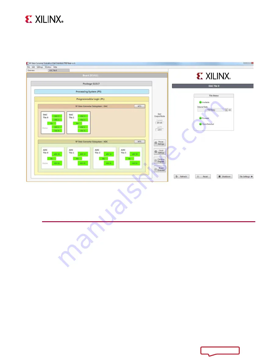
When selecting a tile, the tile status is displayed on the left side as shown in 

Figure 5-2

including the power up state machine’s current state. Controls for 

reset

 and 

shutdown/startup 

are provided. A reset reconfigures the tile to its original bitstream state.

Each individual tile configuration can be accessed by double-clicking the desired tile.

ADC Configuration

The ADC tiles contain the ADCs and supporting signal processing blocks or digital down 

converters (DDCs). There are also clock generators or PLLs in each ADC tile. The GUI 

supports the configuration of all these blocks.

The ADC settings need to be optimized for certain modes of operation. The modes relate to 

where the signal being sampled by the ADC (Fin) lies in relation to the sampling frequency 

(Fs) of the ADCs. As shown in 

Figure 5-3

, the ADC configuration is similar to the RF Data 

X-Ref Target - Figure 5-2

Figure 5-2:

Overview of Tile Status

X21284-090918

Send Feedback

Summary of Contents for UltraScale+

Page 1: ...Zynq UltraScale RFSoC RF Data Converter Evaluation Tool ZCU111 User Guide UG1287 v2018 2 October 1 2018...

Page 2: ...on 2018 2 DAC Data Flow Added information about feeding data to the RF DAC Streaming MUX Added channel control selection information GPIO Selection Replaced Table 3 2 Application Flow Added DDR and BR...

Page 3: ...ata Flow 15 ADC Data Flow 21 Stream Pipes Control and Status Registers 24 GPIO Selection 24 Chapter 4 Clocking Clock Switching 28 Resets 34 Chapter 5 Evaluation Tool System Configuration using the GUI...

Page 4: ...Linux Driver Chapter 9 System Considerations Boot Process 59 Global Address Map 60 Memory 60 Memory Mapping for RF DAC RF ADC 61 Appendix A Reference Design Protocol Specification Commands 62 Example...

Page 5: ...th RF ADCs and RF DACs However one significant benefit is the DACs can be used to provide test signals for the ADC i e loopback which facilitates a very compact and easy to use solution for early demo...

Page 6: ...d for the design Chapter 5 Evaluation Tool System Configuration using the GUI describes the details of system configuration and features supported using the GUI Chapter 6 Software Architecture describ...

Page 7: ...k at up to 6 554 GSPS with an output signal bandwidth of greater than 4 GHz The RF data converters also include power efficient digital down converters DDCs and digital up converters DUCs that include...

Page 8: ...erview DS889 Ref 1 Zynq UltraScale RFSoC Data Sheet DC and AC Switching Characteristics DS926 Ref 2 Zynq UltraScale Device Technical Reference Manual UG1085 Ref 3 X Ref Target Figure 1 2 Figure 1 2 Co...

Page 9: ...t I2C and SD Interface The APU inside the PS is configured to run in symmetric multiprocessing SMP Linux mode The main task of the Linux application is to configure and control the RF ADC and RF DAC b...

Page 10: ...s fed to ADC inputs Digital output of the ADC can be analyzed on the host machine using the GUI DAC to ADC Loopback In this mode the output of the DAC is looped back to the input of ADC In this way yo...

Page 11: ...P Linux Linux frameworks Ethernet Clock Contiguous memory allocator CMA User applications APU Ethernet based server application RFDC driver based features Digital down conversion DDC digital up conver...

Page 12: ...RFSoC Data Converter Evaluation Tool User Guide 12 UG1287 v2018 2 October 1 2018 www xilinx com Chapter 1 Introduction Board specific components Voltage controller Send Feedback...

Page 13: ...linux_bsp PetaLinux board support package BSP is included to build a pre configured SMP Linux image for the APU The BSP includes the following components First stage boot loader FSBL ARM trusted firmw...

Page 14: ...ammable logic PL Figure 3 1 shows the hardware block diagram X Ref Target Figure 3 1 Figure 3 1 Hardware Block Diagram S_AXI_HP0_FPD S_AXI_HP1_FPD M_AXI_HPM0_FPD Programmable Logic Stream Pipe ADC0 Ch...

Page 15: ...which loads the FPGA part when power is switched on The information passed from the host system GUI via Ethernet to the ZCU11 platform is stored in the PL DDR using a DDR controller The application r...

Page 16: ...the corresponding RF DAC channel See GPIO Selection In case of continuous replay from DDR DMA constantly fetches the data and streaming mux switches the channel based on the user selection of enabled...

Page 17: ...ect is asserted based on mode BRAM or DDR For BRAM mode it is controlled by software using GPIOs For DDR mode it is controlled by a hardware logic block channel arbiter The arbiter block allocates the...

Page 18: ...on the Channel Select signal other TREADY signals are ignored X Ref Target Figure 3 4 Figure 3 4 Channel Selection Control Signals Tvalid 0 7 Memory Loopback 0 Memory Loopback 1 Memory Loopback 7 Chan...

Page 19: ...DDR Continuous Playback mode The control switch logic block takes input from PS GPIOs through an EMIO interface and when it is High controlled by software the output of the corresponding control logi...

Page 20: ...rol switch The channel control signal acts as a channel start stop signal This signal exists individually for all channels and can be used to control each channel independently This is done using PS G...

Page 21: ...e of the AXIS FIFO to DMA based on user selection This data is further provided to SG DMA to be stored in PL DDR memory The synchronization among all eight channels is achieved through control switch...

Page 22: ...IO interface that are in turn controlled by software The control switch controls TVALID input to FIFO and TREADY input to ADC I Q Merge Logic The IQ datapath for RF ADC is shown in Figure 3 10 This pi...

Page 23: ...incoming streaming inputs only one streaming data is passed to SG DMA interface based on channel select input X Ref Target Figure 3 10 Figure 3 10 IQ Datapath I Real Stream Q Stream AXIS Broadcaster...

Page 24: ...h_4_fifo_data_count 0x10 Indicates the count inside the FIFO 32 d0 DAC_path_5_fifo_data_count 0x14 Indicates the count inside the FIFO 32 d0 DAC_path_6_fifo_data_count 0x18 Indicates the count inside...

Page 25: ...set 12 ADC1213 FIFO Reset 44 DAC Fabric Filter Select 91 DAC5 Loopback select 13 ADC1213_IQ_Merge_sel 45 DAC3 Channel Control 14 ADC1213 Channel Control 46 DAC6 Loopback select 15 Reserved 47 DAC4 Mem...

Page 26: ...S clocking structure in the ZCU111 evaluation board The RF data converter clocking includes a primary external onboard reference PLL LMK04208 and onboard RF PLLs LMX2594 to generate RF ADC and RF DAC...

Page 27: ...In each Zynq UltraScale RFSoC each RF ADC or RF DAC tile has its own clock input Additionally there is a dedicated input PL SYSREF pin pair per package The PL SYSREF clock is used for multi tile and...

Page 28: ...on MTS mode the streaming interface clocks can be sourced by their respective DAC and ADC tile clocks The switching of the clock is controlled via a clock MUX primitive BUFGMUX see Figure 4 3 and Figu...

Page 29: ...g Clock PCB ADC 1 Analog Clock PCB SYSREF PCB PL SYSREF PCB PL REF CLK PCB MMCM PL CLK Fabric Clock User_sysref_adc User_sysref_dac Fabric Clock PL CLK Example Fs 3 2 GHz Decimation x1 SYREF 8 MHz PL...

Page 30: ...tage Sync logic Channel 4 Control Channel 5 Control N stage Sync logic Channel 6 Control Channel 7 Control ADC 0 Control ADC 1 Control ADC 2 Control ADC 3 Control ADC 4 Control ADC 5 Control ADC 6 Con...

Page 31: ...MHz Figure 4 7 and Figure 4 8 show the RF DAC clock domains Table 4 1 Clock Domains in RF ADC Control and Datapath Logic Block ADC Stream Clock Domain 512 MHz Clock Domain 300 MHz ADC Clock Domain 256...

Page 32: ...ck Converter Loopback Component Loopback Component AXIS FIFO 64 KS AXIS FIFO 64 KS Clock Converter Loopback Component AXIS FIFO 64 KS Clock Converter Loopback Component AXIS FIFO 64 KS To Tile1 channe...

Page 33: ...Tile Control DAC 3 CONTROL Synchronizer Channel 4 Control Channel 5 Control Channel 6 Control Channel 7 Control Synchronizer Synchronizer Synchronizer Tile1 _clk PS Clock Multi Tile Control DAC 4 CONT...

Page 34: ...t register can be accessed Each bit of the register can be used to drive reset to the block appropriately Table 4 3 Reset Distribution in the Evaluation Tool Design Logic Block pl_resetn0 ddr4_sync_rs...

Page 35: ...t AXIS data FIFOs x dac reset_4_n DAC 5 block output AXIS data FIFOs x dac reset_5_n DAC 6 block output AXIS data FIFOs x dac reset_6_n DAC 7 block output AXIS data FIFOs x dac reset_7_n Table 4 3 Res...

Page 36: ...ich can be downloaded for DAC testing and manages the upload of data from the ADCs for analysis in the GUI The GUI shipped with the Xilinx evaluation board supports most of the API functions and confi...

Page 37: ...xternal Component Configuration In the overview tab when clicking on Clock Settings the external PLL can be configured with a set of predefined frequencies as shown in Figure 5 1 When clicking on Powe...

Page 38: ...uration can be accessed by double clicking the desired tile ADC Configuration The ADC tiles contain the ADCs and supporting signal processing blocks or digital down converters DDCs There are also cloc...

Page 39: ...linx com Chapter 5 Evaluation Tool System Configuration using the GUI Converter IP GUI A notable difference is the multi band and complex real settings available in the crossbar setting shown in Figur...

Page 40: ...ter Evaluation Tool User Guide 40 UG1287 v2018 2 October 1 2018 www xilinx com Chapter 5 Evaluation Tool System Configuration using the GUI X Ref Target Figure 5 4 Figure 5 4 ADC Crossbars X21281 0921...

Page 41: ...al or internal PLL sample clock options On chip PLL configuration for internal sample clock generation see Figure 5 5 The configuration of the RF PLLs on the evaluation board for external clocking Not...

Page 42: ...Configuration Like the ADC tiles the DAC tiles contain four DACs Unlike the ADC tiles there is only one configuration The DAC tile contains the same clock generation PLL functionality as the ADC tiles...

Page 43: ...supports coherent sampling The two basic requirements for coherent sampling are The sample clocks for the DAC or external signal generator and ADC are frequency locked This is achieved if the ADC and...

Page 44: ...te action This application is the main interface to the GUI and uses a string based communication protocol described in Chapter 7 Protocol Specification Device drivers expose a systematic interface to...

Page 45: ...d performs appropriate actions RFDC User Space Drivers provide APIs for communication with the RFDC hardware DMA client driver interface dev pl_mem is used to allocate buffer from PL DDR It is also us...

Page 46: ...The DMA client driver uses APIs for this DMA engine The DMA Engine uses the AXI DMA driver to control hardware ina2xx_driver is a Linux driver for ina2xx chips It also provides a sysfs interface for...

Page 47: ...com Chapter 6 Software Architecture Figure 6 2 shows the application execution flow X Ref Target Figure 6 2 Figure 6 2 Application Execution Flow GUI TCP Socket Command Data Protocol Layer Command Ha...

Page 48: ...type and number of arguments and the last argument is the function pointer which needs to be called for the command For the SetMixerSettings command the type of required arguments is uiudduuuu The ty...

Page 49: ...nterface that can be used to call any software API or function Its main purpose is to provide a robust communication method between a host and client application that allows RFDC hardware control comm...

Page 50: ...writedatatomemory command the application receives the number of data bytes from the socket After receiving data samples from the socket the application triggers DMA After DMA is successfully trigger...

Page 51: ...parser parses it If the command is incorrect it returns an error If the command is correct it executes If the execution fails it returns an error with an explicit message If the execution succeeds it...

Page 52: ...ut return format If an input command is not recognized the parser errors out and sends ERROR CMD Invalid Command n If an input command is recognized the parser checks the number of arguments and sends...

Page 53: ...irmware Application TCP Socket TCP Socket sysfs RFdc User Space Driver Libmetal PL Memory Device UIO IIC Client Drivers Clock Power and Power Measurement DMA Client Driver AXI DMA Driver DMA Engine II...

Page 54: ...selected channels Based on this information the firmware creates a bitmask for the selected channels and updates the hardware register so that the hardware knows the enabled channels Depending on the...

Page 55: ...l for all eight DAC pipelines DAC0 to DAC7 o Enables RFDC FIFOs for all eight channels 2 MultiConverter_Init DAC command a Triggers XRFdc_MultiConverter_Init command and returns status This is an RFDC...

Page 56: ...of the DAC channel 4 The firmware prepares the BD chain and triggers the DMA transfer 5 Send the Stop command to reset the currently running DMA transfers before selecting any other mode or sending n...

Page 57: ...hannel by configuring streaming MUX GPIO 4 Enable IQ GPIO if IQ mode is selected 5 Assert external FIFO RESET for corresponding ADC channel 6 Deassert external FIFO RESET for corresponding ADC channel...

Page 58: ...Zynq UltraScale RFSoC Data Converter Bare metal Linux Driver The Linux APIs for the Zynq UltraScale RFSoC Data Converter is described in the Zynq UltraScale RFSoC Data Converter Bare metal Linux Drive...

Page 59: ...esets of the system as well as system power management In the pre configuration stage the PMU executes the PMU ROM and releases the reset of the configuration security unit CSU It then enters the PMU...

Page 60: ...ot process see chapters Programming View of Zynq UltraScale MPSoC Devices and System Boot and Configuration in the Zynq UltraScale MPSoC Software Developer Guide UG1137 Ref 11 and chapter Boot and Con...

Page 61: ...C Partition DDR Start Address Size Component 1 PL 0x410000000 128MB RF DAC RF ADC 2 PL 0x418000000 128MB RF DAC RF ADC 3 PL 0x420000000 128MB RF DAC RF ADC 4 PL 0x428000000 128MB RF DAC RF ADC 5 PL 0x...

Page 62: ...status info to the terminal and should not be used with the Evaluation Tool GUI GetLog None Logged Strings Uses metal_log to return any error warning or informational messages returned from the API or...

Page 63: ...onfigure the PLL sampling rate depending on the source GetLinkCoupling Tile Block Tile Block Mode Get link coupling mode for the requested tile and block SetCoarseDelaySettings Type Tile Block Success...

Page 64: ...with requested frequency SetDACPowerMode board id Tile Block output current Success Fail Configure DAC power GetDACPower Board Tile Board Tile DAC_AVTT DAC_AVCC_AUX DAC_AVCC ADC_AVCC_AUX ADC_AVCC Get...

Page 65: ...neMixerMode CoarseMixerFreq FineMixerScale GetMixerSettings 0 1 2 GetMixerSettings 3 14 Control Path Core Implementation Structure The control path core code is implemented in C code and runs on the A...

Page 66: ...y of unions to allow the same data type to be passed to functions that expect different argument data types The associated wrapper function is called by the function pointer and a return value message...

Page 67: ...ww xilinx com Appendix A Reference Design Protocol Specification This function should be pointed to the method used to actually transmit strings or characters over the desired communication interface...

Page 68: ...to Xilinx documents videos and support resources which you can filter and search to find information To open the Xilinx Documentation Navigator DocNav From the Vivado IDE select Help Documentation an...

Page 69: ...2018 2 zip available at the Zynq UltraScale RFSoC ZCU111 Evaluation Kit site 5 ZCU111 UltraScale RFSoC ZCU111 Evaluation Kit Quick Start Guide XTP490 6 Vivado Design Suite 7 Xilinx Software Developme...

Page 70: ...You may not reproduce modify distribute or publicly display the Materials without prior written consent Certain products are subject to the terms and conditions of Xilinx s limited warranty please re...

Reviews: