


CLM920_TE5 LTE Module Hardware Manual
3
YUGA Information Technology Co.,Ltd
Contents
1 Introduction
....................................................................................................................................................... 7
2 Product Overview
............................................................................................................................................ 7
2.1 General Description
................................................................................................................................. 7
2.2 Key Features
............................................................................................................................................. 8
2.3 Module Function
..................................................................................................................................... 10
3 Application Interface
...................................................................................................................................... 11
3.1 General Description
................................................................................................................................ 11
3.2 Module Interface
..................................................................................................................................... 12
3.2.1 52-pin Goldfinger
............................................................................................................................ 12
3.2.2 Interface definition
.......................................................................................................................... 13
3.3 Power Interface
...................................................................................................................................... 15
3.3.1 Power Design
.................................................................................................................................. 16
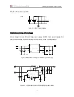
3.3.2 Reference Design of Power Supply
............................................................................................. 17
3.3.3 VDD_EXT 1V8 output
..................................................................................................................... 18
3.3.4 Power-on sequence
........................................................................................................................ 19
3.4 Reset control
........................................................................................................................................... 19
3.4.1 Power off
.......................................................................................................................................... 20
3.5 USB interface
.......................................................................................................................................... 21
3.6 UART interface
....................................................................................................................................... 22
3.7 USIM interface
........................................................................................................................................ 23
3.7.1 USIM card reference circuit
........................................................................................................... 23
3.7.2 UIM_DET Hot-Plug Reference Design
........................................................................................ 24
3.8 General purpose GPIO interface
......................................................................................................... 25
3.9 Network Indication Interface
................................................................................................................. 25
3.10 Analog voice interface
......................................................................................................................... 26
3.10.1 Analog Voice Reference Design
................................................................................................ 26
3.10.2 Analog Voice Reference Design
................................................................................................ 27
3.11 PCM audio interface
............................................................................................................................ 28
3.12 Antenna Interface
................................................................................................................................. 29
4 Overall Technical Indicators
........................................................................................................................ 31
4.1 Overview of this chapter
........................................................................................................................ 31
4.2 Operating frequency
.............................................................................................................................. 32
4.3 Conducted RF Measurements radio frequency
................................................................................. 32
4.3.1 Test environment
............................................................................................................................ 32
4.3.2 Test standards
................................................................................................................................. 33


