


CLM920_TE5 LTE Module Hardware Manual
18
YUGA Information Technology Co.,Ltd
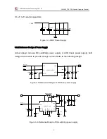
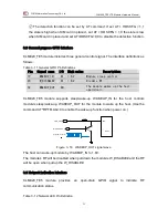
Figure 3- 7 Reference Design of MOS to control the power switch
①
In order to prevent the surge and over voltage damage the module, suggest that
connect a 5.1 V / 500mW zener diode on to the module’s VBAT pin in parallel.
②
Suggest that use another three ceramic capacitors(33pF ,10pF,100nF)near to the
VBAT pin.
③
The minimum working voltage of the module is 3.3V. Due to the peak current will
reach 2.5A while transmit data or call under GSM making a large ripple on the power,
the supply voltage can’t lower than 3.3V.
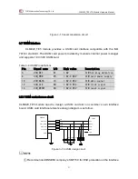
3.3.3 VDD_EXT 1V8 output
The pin 17
th
will output 1.8V after CLM920_TE5 module boots up successfully. Its
maximum current load is 50mA. Using this PIN you can determine whether the module
power-on correctly or not. The VDD_EXT can also be used as external power supply,
such as LED, etc.
G
D
S
10K
470nF
100K
10uF
VBAT
PWR_CTRL
DC_IN


