


CLM920_TE5 LTE Module Hardware Manual
25
YUGA Information Technology Co.,Ltd
②
The detection function can be set by AT command. If set AT + HOSCFG = 1,1
the state is high when SIM card in placed , set AT + HOSCFG = 1,0 the state is low
when SIM card in placed and set AT+HOSCFG=0,0 to disable the detective function.
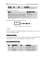
3.8 General purpose GPIO interface
CLM920_TE5 module includes three general control signal. The interface definitions as
follows:
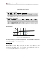
Table 3- 11 General GPIO Pin Definitions
Pin
Signal name
I/O High value
Description
19
WAKEUP_IN
DI 1.8V
Module sleep control
20
W_DISABLE#
DI 1.8V
Disable RF
32
WAKEUP_OUT
DO
The module wakes up the host,
open-drain
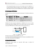
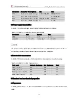
CLM920_TE5 module supports sleep/wake-up. WAKEUP_IN for the host controls
module’s sleep/wake-up, WAKEUP_OUT for the module to wake up the host. (Use the
command AT^RPTFLAG=0 to enable the wake-up function when power on.)
Figure 3- 16 WAKEUP_OUT signal wave
The host can wake-up module by WAKEUP_IN to 1.8V.
The module’s RF will be disabled when pull down the module’s W_DISABLE# and the RF
will be open when pull up the W_DISABLE#.
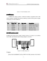
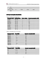
3.9 Network Indication Interface
CLM920_TE5 module provides an open-drain GPIO signal to indicate RF
communication status.
Table 3- 12 Network LED Pin Definition
HOST
INT
Signal Waveform
WAKEUP_OUT
10K
VDD_EXT


