


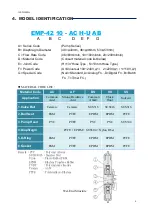
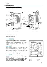
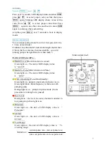


A05G069A
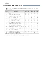
15
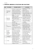
Caution: Unused contacts must avoid short circuits, which may cause inner components to burn
out
Note1
:
1.
Voltage pulse(from 0Vto next 0V as a full cycle, max. pulse=9000 Pulses/min, pulse
width(in mini-second “mSec”) must comply with following table list.
2.
Voltage<0.8V=Low Level; Voltage=3.0V~60V=High Level
Signal
Item
Symbol
Min.
Type
Max.
Unit
Timing
Characteristic
Low time
TA
3.33
∞
mSec
HI time
TB
3.33
∞
mSec
1 Cycle
TC
6.66
∞
mSec
Note2
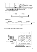
:
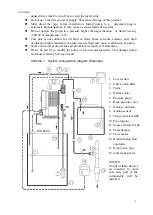
An external switches circuit diagram
Run/Stop Full Speed (switch)
Note3
:
Pulse/Batch/Low level signal connection diagram
:
(Max. power is 20W, overload, short circuit, over voltage or current leads to break
inner devices)
Pin B4
Pin B6
Pin B7
DC_com.
Pin B9,11,13
Pin B8,10,12
Indicator
(Lamp)
MOS switch
DC+ power


