49
RX-V757/DSP-AX757/DSP-AX757SE
RX-V657/HTR-5860
RX-V757/DSP-AX757/DSP-AX757SE
RX-V657/HTR-5860
The condition of ports for model detection
モデル判別ポートの状態
(Not applied to these models. /
このモデルには適用されません。
)
Software version of microprocessor /
マイコンのソフトウェアバージョン
Checksum value of microprocessor /
マイコンのチェックサム
Software modules version of microprocessor /
マイコンのモジュール別ソフトバージョン
O:
Operetion
D:
DSP
X:
XM
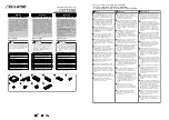
19. SOFTWARE VERSION
ソフトウェアのバージョンおよびチェックサムを表示します。
※図中数値は参考例です。
19. SOFTWARE VERSION
The version and checksum of software are displayed.
* The numeric value in the diagram is for reference.
VER.I039
CHECK
SUM:E8F0
O:25
D:34
X:A7
PORT:00000000
TI
VER.37
TiSUM:B97C3D55
EE
SUM:0000
Software version of DSP /
DSP のソフトウェアバージョン
Checksum value of DSP /
DSP のチェックサム
Checksum value of EEPROM /
EEPROM のチェックサム
(Not applied to these models. /
このモデルには適用されません。
)
20. DSP SOFTWARE REWRITE
DSP のソフトウェア書き換えモードです。
このモデルには適用されません。
20. DSP SOFTWARE REWRITE
The rewriting mode of DSP software.
Not applied to these models.
OSD:
NOTまたはEXISTを選択できます。(SW MODE:
FNC時選択できます。)
YPAO:
NOTまたはEXISTを選択できます。
(SW MODE:
FNC時選択できます。)
OSD: NOT or EXIST can be selected. (SW MODE: Select-
able when FNC has been selected.)
YPAO: NOT or EXIST can be selected. (SW MODE: Select-
able when FNC has been selected.)
18.OSD
:NOT
18.YPAO
:NOT