background image

26

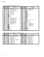
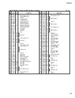
PSR-9000

DP: V410120
FU: V427280

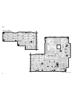
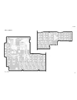
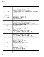
DP Circuit Board

Component side

Component side

CIRCUIT BOARDS

FU Circuit Board

to MK-CN1

to DJACK-CN3

to FDD

to MK-CN2

Pattern side

• CONTENTS

DP Circuit Board

V4101200 (XW156C0)

P26

FU Circuit Board

V4272800 (XV921B0)

P26

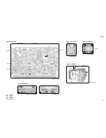
AM Circuit Board

V3558900 (XV931C0)

P27

INV Circuit Board

VY638900 (VT122A0)

P27

EN Circuit Board

V4197300 (XW443B0)

P27

MV Circuit Board

V4197800 (XW438B0)

P27

SCSI Circuit Board

V4271500 (XW083C0)

P27

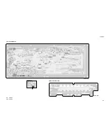
MIC/VR Circuit Board

V4197700 (XW438B0)

P28

MIC/HP Circuit Board

V4197600 (XW438B0)

P28

DM Circuit Board

V4101100 (XW155C0)

P28

AJACK Circuit Board

V4582000 (XV936B0)

P28

VSEL Circuit Board

V4272300 (XW375B0)

P29

NET Circuit Board

V4272100 (XW374B0)

P29

DJACK Circuit Board

V4270600 (XV936B0)

P29

TG Circuit Board

V4101300 (XW157E0)

P30

PN2 Circuit Board

V4197200 (XW443B0)

P30

PN1 Circuit Board

V4197500 (XW443B0)

P32

PN3 Circuit Board

V4197100 (XW438B0)

P34

AMP Conversion Circuit Board

V3727900 (XV922A0)

P36

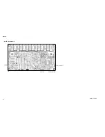
to LCD

to PN3-CN3

to DJACK-CN4

to HDD

to Power transfomer

to SW POWER SUPPLY-CN1

to POWER SWITCH

to AC INLET

to VSEL-CN1

Summary of Contents for Portatone PSR-9000

Page 1: ...WIRING 7 BLOCK DIAGRAM 8 DISASSEMBLY PROCEDURE 9 LSI PIN DISCRIPTION 15 IC BLOCK DIAGRAM 23 CIRCUIT BOARDS 26 TEST PROGRAM 37 POWER ON RESET 40 TROUBLESHOOTING 41 MIDI IMPLEMENTATION CHART 43 PARTS LIST SERVICE MANUAL PK 001628 1 45K Printed in Japan 99 11 ...

Page 2: ...hanges in specification are subject to change without notice or obligation to retrofit Should any discrepancy appear to exist please contact the distributor s Service Division WARNING Static discharges can destroy expensive components Discharge any static electricity your body may have accumulated by grounding yourself to the ground bus in the unit heavy gauge black wires connect to this bus IMPOR...

Page 3: ...armony Echo 17Preset Master EQ 2 Preset 2 User 5 band Part EQ 29 PART 2 band 29 PART R1 R2 R3 LEFT ACMP x 8 SONG x 16 M PAD Touch Response 5 Preset Tempo 32 280 Transpose 24 0 24 Tuning 414 6 440Hz 466 8 Octave 1 0 1 only for Upper Pitch Bend Wheel Modulation Wheel Left Hold Yes AUTO ACCOMPANIMENT Preset 125 Flash 85 max 120 styles or up to 1 8MByte Disk 66 included in the accessory disk DISK DIRE...

Page 4: ... RETURN L L R R TRIM VOL MIC LINE IN LEVEL MIC1 MIC2 LINE INPUT VOLUME Indicator AMPLIFIER 28 W x 2 SPEAKERS Size 13 cm x 2 3 cm x 2 Enclosure Wooden Bass Reex 6 0 liters x 2 POWER SUPPLY Power Consumption 65 W WEIGHT 22 5 Kg 49 lbs 10 oz DIMENSIONS W x H x D 1114 x 464 9 x 182 5 mm without Music Stand 43 7 8 x 18 5 16 x 7 3 16 SUPPLIED ACCESSORIES Music Stand 1 AC Power Cord 1 AC Plug Adaptor 1 i...

Page 5: ... R 2 R S H L H L H L H L H L S L H L M O MODULATION MIC LINE IN INPUT VOLUME MIC LINE IN PHONES PITCH BEND UP DOWN MAX MAX OVER SIGNAL MIC1 MIC2 LINE MIN MIN 1 1 2 3 4 5 6 7 8 9 10 11 13 14 12 16 15 19 17 18 23 21 20 22 POWER ON OFF switch MASTER VOLUME control PITCH BEND wheel MODULATION wheel SONG buttons STYLE buttons ACCOMPANIMENT CONTROL buttons MENU buttons KEYBOARD TRANSPOSE buttons DIGITAL...

Page 6: ...BANK VIEW 1 A B C D E CLICK T S R L M H L M H L H L H M L M H C 1 B E A T NEXT BACK PAGE CONTROL TOUCH SUSTAIN LCD CONTRAST DEMO HARMONY ECHO DSP 4 7 VOICE EFFECT EXIT SLOW FAST POL Y MONO TEMPO D A T A ENTRY 2 3 4 5 6 7 8 ORGAN FLUTES VOCAL HARMONY CUSTOM VOICE UPPER OCTAVE PERCUSSION XG MEMORY REGISTRATION ONE TOUCH SETTING RESET CHOIR PAD SYNTHESIZER SAXOPHONE FLUTE TRUMPET BRASS RIGHT3 GUITAR ...

Page 7: ...3015 1110 11P HDD CN1 PH10P CN4 PH9P Board in Board in Board in AM AMP NET NET Power Supply Unit SW SP conection SPL1 SPR1 SP wire SP SIG FC MDAC Power supply V414500 Power supply 1 JACK FC V524660 AJACK 3 V415370 MKLC 1 V414830 MKLC 2 V414840 MKLC 3 V414850 SCSI V414950 FDD FDD Power supply DJAC FC V523130 VIDEO PN1 PN3 FC INV LCD V415080 LCDC V415170 MIC V526710 VR V414640 PN3 V415130 HP V415190...
Page 8: ...8688M A0 8 D0 15 A0 8 D0 15 D0 31 A0 8 D0 15 D0 15 D0 15 D0 15 D16 31 Mask ROM 64Mbit D0 15 SWP30 Master SWP30 Slave Lo Addres Hi Data Lo Data Hi Address D0 5 A18 24 A18 24 A1 21 D0 31 MEL CLOCK MEL CLOCK IRQ AUX IN L L R R MUTE 5BAND EQ 22 24V A0 21 D0 15 Main CPU SH7043 D0 31 D0 31 A0 21 D0 7 D0 7 D0 7 A0 21 D0 31 D0 15 82C51 BACKLIGHT CN CN D0 7 D0 7 D0 15 D0 7 D0 7 PIF32 IRQ ROM INVERTER INVER...

Page 9: ...oard 700a Bind Head Tapping Screw B 3 0X10 MFZN2BL EP600140 8 DJACK Circuit Board 700b Bind Head Tapping Screw B 3 0X10 MFZN2BL EP600140 10 SCSI Circuit Board 730 Pan Head Screw 2 5X6 MFZN2BL VS206600 2 PITCH BEND Wheel 480c Bind Head Tapping Screw B 3 0X8 MFZN2Y EP600250 2 MODULATION Wheel 480d Bind Head Tapping Screw B 3 0X8 MFZN2Y EP600250 2 AM Circuit Board 40a Bind Head Tapping Screw B 3 0X10...

Page 10: ...ard can then be removed Fig 4 6 INV Circuit Board 6 1 Remove the lower case See procedure 1 6 2 Remove the power supply unit See procedure 2 6 3 Remove the four 4 screws marked 70b and INV cover The INV circuit board can then be removed Fig 4 3 AMP Circuit board 3 1 Remove the lower case See procedure 1 3 2 Remove the power supply unit See procedure 2 3 3 Remove the two 2 screws marked 50a The pow...

Page 11: ...8 1 Remove the lower case See procedure 1 8 2 Remove the power supply unit See procedure 2 8 3 Remove the left and right speaker box units See procedure 7 8 4 Remove the four 4 screws marked 60 The woofer can then be removed Fig 5 9 Tweeter 9 1 Remove the lower case See procedure 1 9 2 Remove the power supply unit See procedure 2 9 3 Remove the left and right speaker box units See procedure 7 9 4 ...

Page 12: ...MV circuit board can then be removed Fig 6 13 INLET Circuit Board and VSEL Circuit Board 13 1 Remove the lower case See procedure 1 13 2 Remove the power supply unit See procedure 2 13 3 Remove the left speaker box unit See procedure 7 13 4 Remove the two 2 screws marked 480f and the POWER knob The power switch can then be removed 13 5 Remove the two 2 screws marked 700c The INLET circuit board ca...

Page 13: ...ard and TG circuit board See procedure 15 17 4 Remove the AM circuit board See procedure 2 17 5 Remove the AM shield cover See procedure 16 17 6 Remove the eighteen 18 screws marked 5 The MK circuit board can then be removed Fig 8 Fig 8 5 Bind Head Tapping Screw S 3 0X10 MFZN2Y EP630630 50d x 3 40g x 2 40e x 5 40g x 2 40f x 3 Fig 7 40 Bind Head Tapping Screw B 3 0X8 MFZN2Y EP600250 50 Bind Head Ta...

Page 14: ... circuit board can then be removed Fig 9 20 PN2 Circuit Board 20 1 Remove the lower case See procedure 1 20 2 Remove the power supply unit See procedure 2 20 3 Remove the left and right speaker box units See procedure 7 20 4 Remove the DP circuit board See procedure 14 20 5 Remove the DM circuit board and TG circuit board See procedure 15 20 6 Remove the keyboard assembly See procedure 16 20 7 Rem...

Page 15: ...2 73 74 75 76 77 78 79 80 VDD L1RAS2 L1RAS3 GND HDRAS0 HDRAS1 GND VDD LDRAS0 LDRAS1 LMA1 LMA0 GND LMA1X LMA0X GND VDD HMA1 HMA0 HMA1X HMA0X D0 D1 GND D2 D3 D4 D5 A2 WRN GND VDD CSN A0 A1 MCLK SYI HBANK LBANK REFRN O O O O O O I I O O I I O O I I I I I I I I I I I I I O O O RAS2 for LoMem SIMM 1 RAS3 for LoMem SIMM 1 RAS for HiMem DRAM 0 RAS for HiMem DRAM 1 RAS for LoMem DRAM 0 RAS for LoMem DRAM ...

Page 16: ...r supply Data bus Ground 73 74 75 76 77 78 79 80 81 82 83 84 85 86 87 88 89 90 91 92 93 94 95 96 97 98 99 100 101 102 103 104 105 106 107 108 109 110 111 112 113 114 115 116 117 118 119 120 121 122 123 124 125 126 127 128 129 130 131 132 133 134 135 136 137 138 139 140 141 142 143 D15 D14 D13 D12 VCC D11 VSS D10 D9 D8 D7 D6 VCC D5 VSS D4 D3 D2 D1 D0 VSS XTAL MD3 EXTAL MD2 NMI VCC PA16 PA17 MD1 MD0...

Page 17: ... 141 142 143 144 145 146 147 148 149 150 151 152 153 154 155 156 157 158 159 160 161 162 163 164 165 166 167 168 169 170 171 172 173 174 175 176 177 178 179 180 181 182 183 184 185 186 187 188 189 190 191 192 193 194 195 196 197 198 199 200 201 202 203 204 205 206 207 208 209 210 211 212 213 214 215 216 217 218 219 220 221 222 223 224 225 226 227 228 229 230 231 232 233 234 235 236 237 238 239 240...

Page 18: ...95 96 97 98 99 100 101 102 103 104 105 106 107 108 109 110 111 112 113 114 115 116 117 118 119 120 121 122 123 124 125 126 127 128 129 130 131 132 133 134 135 136 137 138 139 140 141 142 143 144 145 146 147 148 149 150 151 152 153 154 155 156 157 158 159 160 SO7 SO6 SO5 VDD VSS SO4 SO3 SO2 SO1 SO0 WDCK SWPKON IRQN VDD VSS XTAL_I XTAL_O MCLK VDD VSS MICN CLKIN SYWIN SYW SYWD VDD VSS CLKO WCLK HCLK ...

Page 19: ...chain clock Data bus shift clock Ground X driver latch pulse Frame signal for X Y driver Power down signal for displaying off mode Scan start signal Scan shift clock VRAM data bus VRAM address bus Not used SED1335F0B XQ595A00 LCDC LCD Controller DP IC4 PIN No NAME I O FUNCTION PIN No NAME I O FUNCTION 1 2 3 4 5 6 7 8 9 10 11 12 13 14 15 16 17 18 19 20 21 22 23 24 D5 D6 D7 IRQ0 IRQ1 VSS6 IRQ2 IRQ3 ...

Page 20: ...F AD0 AD1 S0 I I I O I I I I O O O O O O O O O O O O O O O O O O O O I I I Switch matrix data MIDI transmit data Switch matrix data LED drive data LED and switch drive data Grounded Analog input Analog input Switch matrix data MN101C027YB XS711200 CPU EN IC1 PIN No NAME I O FUNCTION PIN No NAME I O FUNCTION 1 2 3 4 5 6 7 8 9 10 11 12 13 14 D2 D3 RXD GND D4 D5 D6 D7 TXC WR CS C D RD RXRDY I I I I I...

Page 21: ...ndex signal Read data input from FDD Clock Clock Ground Power supply Write control Writ data to FDD Ground Step signal to control head of FDD Direction Head load Head select Ground Drive select Ground Motor on Ground HD63266F XI939A00 FDC Floppy Disk Controller DP IC17 PIN No NAME I O FUNCTION PIN No NAME I O FUNCTION 1 2 3 4 5 6 7 8 9 10 11 12 13 14 LRCK DATA BCK CLKO XTI XTO DGND VDD Vcc2R AGND2...

Page 22: ... ROUT0 O O O O O O O O O O O O O O O O O O O O O O O O O O O O Read strobe High Low Write strobe High Low Ground Out buffer Address bus Ground Out buffer 5 V Address bus Sync signal output Ground Out buffer SC_NTSC signal output SC_PAL signal output Ground Out buffer Color data 1414 AAPI XV481B00 GATE ARRAY Video Out DP IC8 PIN No NAME I O FUNCTION PIN No NAME I O FUNCTION 1 2 3 4 5 6 7 8 9 10 11 ...

Page 23: ...request Chip select Power supply 5V Port DMA acknowledge Port read Port write Port DMA request Ground Port DMA data bus Power supply 5V Ground 51 52 53 54 55 56 57 58 59 60 61 62 63 64 65 66 67 68 69 70 71 72 73 74 75 76 77 78 79 80 81 82 83 84 85 86 87 88 89 90 91 92 93 94 95 96 97 98 99 100 LVDD PD13 PD2 PD12 PD3 VSS PD11 PD4 PD10 PD5 HVDD PD9 PD6 PD8 PD7 VSS XSIO XSREQ VSS XSCD XSSEL VSS XSMSG ...

Page 24: ...3Y Vss 14 13 12 11 10 9 8 VDD 6A 6Y 5A 5Y 4A 4Y 1 A 2 3 4 5 6 7 8 9 V IN V IN OUT A A A V IN IN OUT B B B B 1 2 3 4 V 8 7 6 5 Output A V Non Inverting Input A DC Voltage Supply DC Voltage Supply Output B Inverting Input B Non Inverting Input B Inverting Input A 1 2 8 9 VC1 VC2 VCC In 7 Amp Out GND 4 VC4 3 VC3 6 VC5 5 amp 1 2 3 4 5 6 7 IN1 NF1 IN2 NF2 IN3 NF3 IN4 16 15 14 13 12 11 10 Vcc GND Vcc OU...

Page 25: ...G 1A 1B 1Y0 1Y1 1Y2 1Y3 GND 1 2 3 4 5 6 7 8 9 10 11 12 13 14 15 16 Vcc 2G 2Y2 2Y0 2A 2B 2Y1 2Y3 1 D1R 2 3 4 5 6 7 8 9 10 A1 A2 A3 A4 A5 A6 A7 A8 GND 11 12 13 14 15 16 17 18 19 20 VCC G B1 B2 B3 B4 B5 B6 B7 B8 1 2 3 4 5 6 7 1B 1A 1R 1DE 2R 2A 2B 16 15 14 13 12 11 10 Vcc 1D 1Y 1Z 2DE 2Z 2Y 8 GND 9 2D TC74VHC32F TEL XR337A00 OR TG IC18 28 40 DM IC19 34 DP IC6 TC74VHC74F XN964A00 D FF DM IC18 Vcc 2CLR...

Page 26: ...271500 XW083C0 P27 MIC VR Circuit Board V4197700 XW438B0 P28 MIC HP Circuit Board V4197600 XW438B0 P28 DM Circuit Board V4101100 XW155C0 P28 AJACK Circuit Board V4582000 XV936B0 P28 VSEL Circuit Board V4272300 XW375B0 P29 NET Circuit Board V4272100 XW374B0 P29 DJACK Circuit Board V4270600 XV936B0 P29 TG Circuit Board V4101300 XW157E0 P30 PN2 Circuit Board V4197200 XW443B0 P30 PN1 Circuit Board V41...

Page 27: ...d Component side to MV CN301 to AJACK CN102 to AJACK CN101 to AMP CN1 to AM CN3 to PN1 CN2 C0001 L0001 R0002 R0001 TR001 L0002 C0002 TR002 CN001 1 2 3 4 5 6 7 8 9 10 11 12 MV Circuit Board Component side SCSI Circuit Board Component side Pattern side to TG CN5 to TG CN4 CN002 to LCD to TG CN3 to DM CN7 E 12 26 2 1 49 50 24 25 2 1 50 49 CN2 CN1 P18 V0 ...

Page 28: ... Board to PITCH MODU WHEEL to DJACK CN1 MIC VR Circuit Board to MIC HP CN101 Component side Component side E to AM CN5 to TG CN7 to MIC VR CN201 to SICI CN2 to PN1 CN1 to DJACK CN2 to MK CN1 R L L R R TRIM L L R R 1 2 L L R LOOP SEND AUX IN LOOP RETURN LINE OUT to AM CN6 to AM CN7 to TG CN6 to TG CN11 MIC LINE select INPUT VOLUME PHONES MIC LINE IN ...

Page 29: ...ide Component side DJACK Circuit Board E B P E VSEL Circuit Board NET Circuit Board Component side Component side SWITCH 1 VOLUME FOOT PEDAL to DM CN1 IN OUT MIDI A PC KEYBARD SWITCH 2 IN OUT MIDI B HOST SELECT VIDEO OUT TO HOST to DM CN5 to DP CN7 to DP CN6 to Speaker to AMP CN3 to FU CN5 ...

Page 30: ...e Component side PN2 Circuit Board 1 2 3 4 5 6 7 8 EXIT TEMPO DATA ENTRY DIRECT ACCESS MAIN MIXER PART ON OFF PART to PN3 CN2 to PN1 CN3 to INV CN1 to FDD to Power supply CN2 to AM CN2 to MIC HP CN102 to AM CN1 N C to DM CN6 N C Pattern cut Connection cut Jamper wire ...

Page 31: ...31 PSR 9000 TG V410130 PN2 V419720 TG Circuit Board Pattern side Pattern side PN2 Circuit Board Pattern cut cut ...

Page 32: ...I VII MIDI FUNCTION DISK SCSI MIXING CONSOLE DIGITAL RECORDING SOUND CREATOR C B A E D STOP 3 2 1 4 D SONG SETUP V IV III II I DANCE 16 BEAT 8 BEAT AUTO ACCOMPANIMENT SONG PLAYER COUTRY R B SWING JAZZ BALLROOM MARCH WALTZ LATIN III II I B A TAP C A A A A to PN3 CN1 to EN CN201 to PN2 CN101 to DM CN4 N C ...

Page 33: ...33 PSR 9000 PN1 V419750 PN1 Circuit Board Pattern side A A A A ...

Page 34: ... 4 5 6 7 MUSIC DATABASE BACK NEXT F G H I J DEMO LCD CONTRAST SUSTAIN TOUCH SLOW FAST DSP 4 7 POLY NONO HARMONY ECHO CUSTOM VOICE ORGAN FLUTES V H 9 DSP 8 TALK MEMORY CUSTOM VOICE ORGAN FLUTES XG PERCUSSION SYNTHESIZER CHOIR PAD FLUTE SAXOPHONE BRASS TRUMPET R1 R1 R2 R2 R3 R3 7 8 SELECT MIC SETUP A A A A to PN1 CN4 to DP CN5 to PN2 CN102 N C ...

Page 35: ...35 PSR 9000 PN3 V419710 PN3 Circuit Board Pattern side A A A A ...

Page 36: ...36 PSR 9000 AMP V372790 AMP Circuit Board Component side to NET CN1 to Power transformer to AM CN4 B ...

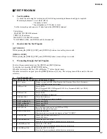
Page 37: ... the next selection 4 Test Program List No LCD display Test Functions and Judgment Criteria 1 001 Version Displays version for ROM Main Program Sub Program Wave Style Parameter Displays the flash memory protect state 2 002 Rom Chk1 Checks ROMs MAIN Program ROM SUB Program ROM Voice Parameter ROM Style ROM For NG ROM name is displayed 3 003 Ram Chk1 Checks RAMs For NG RAM name is displayed 4 004 Fl...

Page 38: ... PHONES R less than 50 dBm AUX OUT L L R 19 2 dBm 3 dB AUX OUT R less than 40 dBm LOOP SEND L L R 11 3 dBm 3 dB LOOP SENDER R less than 70 dBm SUB1 less than 50 dBm SUB2 less than 50 dBm 21 021 Oputput Sub1 Check the Sub1 output level 1 kHz PHONES L less than 65 dBm PHONES R less than 65 dBm AUX OUT L L R less than 70 dBm AUX OUT R less than 70 dBm LOOP SEND L L R less than 70 dBm LOOP SENDER R le...

Page 39: ...t is at maximum 50 050 ModWheelChk Check that the C3 note sound is produced when the MODULATION wheel is at minimum and the C4 note sound is produced when it is at maximum 51 051 ExpPedal Chk Connect the foot pedal into the VOLUME terminal Check that the C3 note sound is produced when the foot pedal is at minimum and the C4 note sound is produced when it is at maximum 52 052 AfterTouch Chk Check t...

Page 40: ... following specifications PHONES L R less than 65 dB 5 3 MIC LINE Input Level Level Indicate LED When the following input level are used with test program number 055 confirm that output levels are as follows V 1 00 MIC LINE Input level Output level SIGNAL LED OVER LED LINE 56 0 dBm 10 0 dBm 3 dB OFF OFF MIC 2 56 0 dBm 0 4 dBm 3 dB ON OFF MIC 1 50 0 dBm 12 8 dBm 3 dB ON ON V 1 10 MIC LINE Input lev...

Page 41: ...robably exceeding the maximum polyphony of the PSR 9000 The PSR 9000 can play up to 126 notes at the same time including voice R2 voice R3 voice L auto accompaniment song and multi pad notes When the maximum polyphony is exceeded the earliest played notes will stop sounding letting the latest played notes sound This is re ferred to as last note priority The accompaniment or song does not play back...

Page 42: ...mpaniment chord does not change even when a different chord is played or the chord is not recognized Are you sure you re playing on the left hand section of the keyboard You may be using single finger type fingering in the fingered mode or vice versa Use the correct type of chord fingering for the selected auto accompaniment fingering mode The displayed disk free area value does not coincide with ...

Page 43: ...al Time Commands o o Aux All Sound OFF x o 120 126 127 ResetAllCntrls x o 121 ResetAllCntrls x o 121 Local ON OFFx x All Notes OFFx o 123 125 Mes Active Sense o o sages Reset x x Notes 1 2 3 see next page Mode 1 OMNI ON POLY Mode 2 OMNI ON MONO o Yes Mode 3 OMNI OFF POLY Mode 4 OMNI OFF MONO x No Default 3 3 Mode Message x x Altered x 0 32 o o 1 Bank Select 1 5 7 10 11 o o 1 6 38 o o 1 Data Entry ...

Page 44: ...ASTER TUNE XG System parameter MASTER TUNE XG System paramerer TRANSPOSE System exclusive messages which change the REVERB CHORUS or DSP EFFECT settings XG MULTI EQ parameters Also the MIDI messages affect the panel settings when one of the following MIDI reception modes is selected These modes can be selected on the panel RIGHT1 RIGHT2 RIGHT3 LEFT KEYBOARD ACMP RHYTHM1 ACMP RHYTHM2 ACMP BASS ACMP...

Page 45: ...t model Y Export model A Australian model B British model C Canadian model E European model H North European model I Indonesian model WARNING Components having special characteristics are marked and must be replaced with parts having specification equal to those originally installed The numbers in QTY shows quantities for each unit The parts with in Parts No are not available as spare parts The ma...

Page 46: ...ind Head Tapping Screw 1 ACCESSORIES Music Rest Assembly AC Cord Set AC Cord Set AC Cord Set Connector Floppy Disk E U N E N U C61K6 S 72B L 50 3 0X8 MFZN2Y 4 0X10 MFZN2Y MKLC 1 MKLC 2 MKLC 3 3 5X12 0 8 MFZN2 AM AM MDAC POWER 2 L 470 UPPER DM DP TG LOWER LEFT RIGHT 4 0X14 MFZN2Y E U N 4 0X12 MFZN2Y BL T1 6 3 0X4 MFNI33 3 0X8 MFZN2BL BK 1 12X50 3 0X8 MFNI33 3 5X16 MFZN2BL E 2P 2 5m U2P 2 44m 7A B 2...

Page 47: ...3 PSR 9000 Upper Case Top View 420 LCD Assembly See page 19 Lower Case Bottom View 380 390 370 340 310 340 340a ...

Page 48: ... 1 Speaker Unit L See page 21 430 380 260 350 360 320 330 Lower Case Insid View 2 30 40 110 290 280 110 290 110 290 270 290 300 310 310 300 290 210 440 220 40 230 170 180 40 160 Speaker Unit R See page 21 Power Supply Unit See page 22 ...

Page 49: ...T NET 13 0cm 8 ohm 50 W 3 0cm 8 ohm 25 W 3 5X16 MFZN2BL 3 5X20 MFZN2BL PE PE S 72B L 50 PE ス ピ ー カ ユ ニ ッ ト ス ピ ー カ ユ ニ ッ ト L ス ピ ー カ ユ ニ ッ ト R ボックス L 木部集成 ボ ッ ク ス R 木 部 集 成 基 板 サ ポ ー ト N E T シ ー ト ス ピ ー カ ス ピ ー カ ス ピ ー カ 固 定 金 具 B ス ピ ー カ 固 定 金 具 A バ イ ン ド T P 1 種 バ イ ン ド T P 1 種 防 振 フ ォ ー ム 目 隠 し フ ォ ー ム ア ー ス 線 1 2 束 線 止 め 防 振 フ ォ ー ム PSR 9000 V393870 V427120 V437450 V387380 V510380 V510390 V523...

Page 50: ...80 150 170 160 120 110 100 80 70 60 50 30 570 580 590 600 700 710 720 730 690 700 660 670 680 700 610 620 630 640 700 550 480 550 480 550 480 480 440 550 480 530 520 510 480 650 480 420 410 400 370 490 790 490 490 480 490 780 490 480 380 370 360 350 340 480 470 460 400 480 380 360 390 500 480 540 480 320 330 230 140 210 140 190 740 190 130 90 40 20 10 40 440b 440 450 670 440 660 680 Fig B Refer to...

Page 51: ...パ ワ ー ス イ ッ チ カ バ ー ボ リ ュ ー ム ク ロ ス M V シ ー ト V R 束 線 バ イ ン ド B タ イ ト バ イ ン ド B タ イ ト 束 線 止 め 束 線 止 め PSR 9000 E B V364810 U V364830 N V364820 SONG I V SONG SETUP STYLE 8BEAT COUNTRY SONG PLAYER AUTO ACCOMP STYLE LATIN DISKDIRECT VOICE PIANO CUSTOM V ACCOMP CONTROL INTRO TAP TEMPO ACCOMP CONTROL MAIN VARIATION ACCOMP CONTROL ENDING FADE IN OUT ACCOMP CONTROL FILL IN BREAK MENU DISK SCSI MIDI KEYBO...

Page 52: ...CRIPTION REMARKS QTY RANK 部 品 名 1 1a 1b 1b 1b 1b 1b 1b 1c 1d 1e 1f 2 3 4 5 6 VN399200 VL570000 VL570100 VL570200 VL570300 VL570400 VL570500 VL570600 VC077600 VR857100 VN406100 V I 9 1 2 0 0 0 VF834100 VM630100 EP630630 VC079800 KEYBOARD ASSEMBLY Keyboard Assembly MK Frame Assembly MK Frame White Key White Key White Key White Key White Key White Key Black Key Spring Felt PC Sensor Circuit Board Rub...

Page 53: ...older FDD Holder FDD Bonding Head Screw Bushing Adhesive Tape Connector Assembly Connector Assembly MF355F 3252MG F RIGHT LEFT 3 0X6 MFNI33 ECT 590S W 15 FDD POWER FDD F D D A S S Y F D D A s s y 3 5 F D D F D D 固 定 金 具 R F D D 固 定 金 具 L ボ ン デ イ ン グ コ ネ ジ ゴ ム ブ ッ シ ュ 綿 粘 着 テ ー プ F D D 電 源 束 線 F D D 束 線 PSR 9000 V364880 V387660 V387670 ZL35000 16 01 01 05 4 4 10 80 70 20 30 60 50 40 60 20 30 Top Vi...

Page 54: ...10 PSR 9000 POWER SUPPLY UNIT Bottom Open View Power Supply Unit Assembly Top Open View 50 50 30 110 120 130 150 170 160 210 40 50 100 230 220 190 100 180 200 20 50 80 90 70 10 50 60 110 120 130 140 ...

Page 55: ...d Circuit Board Connector Assembly Connector Assembly Saddle Cord Holder Adhesive Tape Cord Binder INV Bush Braizer W H Tap Screw E U N UPPER LOWER 3 0X6 MFZN2Y FU E GBR FU U CSA FU N POW2 A POW2 B SWP CE U CS POWER 1 E ICE65 E UL CSA A N ICE65 E 4 0X14 MFZN2Y AMP E GBR N AMP U CSA SP RELAY SIG EDS 17L BK 1 19X70 S 72B L 50 3 0 X 6 MFZN2Y 電 源 ユ ニ ッ ト 電 源 ユ ニ ッ ト 電 源 ユ ニ ッ ト 電 源 ユ ニ ッ ト 電 源 カ バ ー U...

Page 56: ...top Ring Rotary Variable Resistor Connector Assembly Cord Holder GND Wire 7 12 10 0K RK163111 WL L 1070 BK 1 ホ イ ー ル A S S Y ホ イ ー ル A s s y フ レ ー ム ホ イ ー ル リ タ ー ン S P ホ イ ー ル チ ュ ー ブ C S 形 止 め 輪 ロ ー タ リ ー V R W L 束 線 イ ン シ ュ ロ ッ ク タ イ ア ー ス 線 7 PSR 9000 V387620 V453380 PITCH MODULATION PITCH MODULATION V414540 V522980 03 01 04 01 03 01 2 2 3 2 2 Modulation Wheel Pitch Bend Wheel 80 20 40 30 50 1...

Page 57: ...ectrolytic Cap Electrolytic Cap Electrolytic Cap AM AMP E GBR N AMP U CSA DM DP EN PN1 PN2 FU E GBR FU U CSA FU N INLET INLET INV DJACK AJACK LC MV MIC VR MIC HP PN3 NET SCSI TG VSEL AM 0 55 PH 10P TE XH 4P TE PH 8P TE PH 9P TE PH 7P TE PH 14P TE PH 4P TE 1SS133 1SS176 1SS133 1SS176 2SK105 E F 2SK105 E F UPC4570HA UPC4570HA LA6517 UPC4570HA UPC4570HA DC MR82 12USR 2SC1740S R S 2SC1740S R S 2SA933S...

Page 58: ...0 0 1 4 J 680 0 1 4 J 1 0K 1 4 J 4 7K 1 4 J 10 0K 1 4 J 18 0K 1 4 J 22 0K 1 4 J 27 0K 1 4 J 33 0K 1 4 J 47 0K 1 4 J 56 0K 1 4 J 82 0K 1 4 J 100 0K 1 4 J 560 0K 1 4 J AMP E GBR N AMP U CSA 3 0X12 MFZN2Y 3 0X20 MFZN2Y PC PH1 30BS172H L80 0 55 PH 9P TE VH 3P TE VH 4P TE 11ES4 D3SBA20 4103 4 0A 5 00A S 5 00A JU 5 00A S 5 00A JU STK401 040 M5227P M5227P 0 55 0 55 0 55 0 55 0 55 0 55 DC G5Z 2A YA 2SC181...

Page 59: ...1 2K 1 4 J 3 3K 1 4 J 3 9K 1 4 J 5 6K 1 4 J 6 8K 1 4 J 10 0K 1 4 J 15 0K 1 4 J 22 0K 1 4 J 100 0 1 4 J 10 0 1W J DM DICF 42CS E PH 5P SE PH 4P SE 53014 3P TE PH 9P SE PH 8P SE TX25 80P LT H1 HIF3FC 50PA2 54DSA TX25 80P 12ST H1 PH 2P TE MA221 MA221 RB100A T 32 RB100A HD6437043AE00F KM416C1200CJ 6 KM416C1200CJ 6 TC74VHC04F TC74VHC08F 28F160S5 28F160S5 IC PST591DMT TC74VHC245F TC74VHC245F TC74VHC11F ...

Page 60: ... T 560J 56U LEM2520 T 560J 0 0 0 0 J 0 0 0 0 J 0 22U LEM2520TR22K 0 0 0 0 J 0 0 0 0 J SMD100 2018 2 SMD 7M SMD 49 10M SMD 49 22 5M SMD 49 100 6 3V 100 16V 1 50V 3 3 50V 5P 50V C 27P 50V J 100P 50V J 470P 50V J 0 01 50V K 0 1 16V Z 0 63M J 56 0 1 4 J 68 0 1 4 J 100 0 1 4 J 180 0 1 4 J 820 0 1 4 J 47 0 1 4 J 100 63M J 220 63M J 680 63M J 1 0K 63M J 3 3K 63M J 6 8K 63M J 10K 63M J 100K 63M J 470K 63M...

Page 61: ...HC245F TC74VHC245F TC74HC245AF TC74VHC11F EL HD63266F 56U LEM2520 T 560J 56U LEM2520 T 560J 0 22U LEM2520TR22K 56U LEM2520 T 560J 0 22U LEM2520TR22K 56U LEM2520 T 560J 56U LEM2520 T 560J 0 22U LEM2520TR22K 2SA1020 Y TPE6 Y 2SA1162 O Y 2SC2712 Y 2SC2412K Q R S 2SC2412K Q R S 8M CSTCC8 00MG 14 318MHZ DSX151G 17 734MHZ DSX151G 6 144MHZ SMD 49 16M CSACS16 00MX24 5P 50V C 10P 50V D 15P 50V J 18P 50V J ...

Page 62: ...133 1SS176 1SS133 1SS176 REB161 PVB 15F MN101C027YB TD62083CP TD62785P SOURCE SLZ290B 03 T2 GR SLZ290B 03 T2 GR SLZ 174B 03 T1 RE SLZ 174B 03 T1 RE SLZ290B 03 T2 GR SLZ290B 03 T2 GR SLZ 190B 03 RE SLZ 190B 03 RE SLZ 174B 03 T1 RE SLZ 274B 03 T1 GR SLZ 274B 03 T1 GR SLZ 290B 17 T1 GR SLZ 190B 17 T1 RE SKQNAJ SKQNAJ SKQNAJ SKQNAJ DTC123JS TP DTC123JS TP DTB123YS TP 8 00M EFOMC8004T4 8 00M EFOMC8004A...

Page 63: ...4700P 250V J U C S INLET CCT9302 0101M VA 2P TE INV 0 068 250 ECQE26 18P 3KV J XH 2P SE 53259 4P SE LH L 08TB221K CLF16A 2SC3669 O Y TPF2 2SD1863 TV2 82 390 2SC3669 O Y TPF2 2SD1863 TV2 82 390 5 6K 1 4 J DJACK AJACK 0 55 3 0X10 MFZN2BL PH 5P TE PH 8P TE PH 4P TE PH 2P TE PH 14P TE PH 4P TE PH 3P TE 1SS133 1SS176 1SS133 1SS176 6N137 6N137 SN75C1168N SN74HCU04N HLJ7001 01 YKB21 5012 BL YKB21 5012 BL...

Page 64: ...R200QNT SBT 0180W SBT 0180W FL5R200QNT BL02RN2 R62T4 FL5R200QNT FL5R200QNT BL02RN2 R62T4 FL5R200QNT SSSF144 S06N 0 B 10K RK09K12A0 BL02RN2 R62T4 BL02RN2 R62T4 FL5R200QNT FL5R200QNT 220P 50V K 1000P 50V K 0 01 50V Z 47 00 6 3V 4 7 50 0V 10 00 16 0V 1 00 50 0V 0 1 25V Z 100 0 1 4 J 220 0 1 4 J 1 0K 1 4 J 10 0K 1 4 J 22 0K 1 4 J 470 0K 1 4 J LC 24mm 330m 0 55 53014 11P TE 53014 12P TE 53014 3P TE 1SS...

Page 65: ... GR SLZ 174B 03 T1 RE SLZ 190B 03 RE SLZ290B 03 T2 GR SKQNAJ SKQNAJ SSSF025000 ERTD2ZGJ202T 2K 2SC1740S R S B 10K RK09K1130A5R A 10 0K RK09K12C A 10 0K RK14K12C0 BL02RN2 R62T4 BL02RN2 R62T4 MTZJ4 3B 4 3V 220P 50V K 2700P 50V K 8200P 50V K 0 01 50V Z 100P 50V J 0 1 25V Z 1 000 25V Z 1 00 50 0V 100 00 25 0V 100 0 1 4 J 150 0 1 4 J 220 0 1 4 J 1 0K 1 4 J 1 2K 1 4 J 3 3K 1 4 J 5 6K 1 4 J 10 0K 1 4 J 2...

Page 66: ...CM1716E PCM1716E MSM514260C 60TS K HD74LVC138FP MSM514260C 60TS K UPC2933T E1 UPC2933T E1 HD6437043AE00F TC203C760HF 002 LB1443N UPC4570G2 AK5351 VF E2 D65621GF 028 3B9 MSM514260C 60TS K TC74VHC32F TEL TC74VHC245F TC74VHC245F TC74VHC08F 28F400B5 28F400B5 TC74VHC08F TC74VHC32F TEL TC74VHC245F TC74VHC245F MX23C1610PC 10 TC74VHC245F TC74VHC245F MSM514260C 60TS K MSM514260C 60TS K TC74VHC32F TEL MX23C...

Page 67: ...M J 470K 63M J VSEL 3 0X10 MFZN2BL VH 5P SE HXW0131 01 910 E ICE65 E UL CSA A N ICE65 E E 2P 2 5m U2P 2 44m 7A B 2P 2 5m CCT5902 SDDLB1216A J U C S EDMMPU3BCF MF355F 3252MG F チ ッ プ ケ ミ コ ン チ ッ プ ケ ミ コ ン チ ッ プ ケ ミ コ ン チ ッ プ ケ ミ コ ン チ ッ プ ケ ミ コ ン チ ッ プ ケ ミ コ ン チ ッ プ セ ラ C H チ ッ プ セ ラ S L チ ッ プ セ ラ S L チ ッ プ セ ラ S L チ ッ プ セ ラ B チ ッ プ セ ラ F チ ッ プ 抵 抗 チ ッ プ 抵 抗 チ ッ プ 抵 抗 チ ッ プ 抵 抗 チ ッ プ 抵 抗 チ ッ プ 抵 抗 チ...

Page 68: ...0 VT695100 Speaker Speaker Power Supply Unit Power Transformer Power Transformer Power Transformer Rotary Variable Resistor 13 0cm 8 ohm 50 W 3 0cm 8 ohm 25 W E ICE65 E UL CSA A N ICE65 E 10 0K RK163111 ス ピ ー カ ス ピ ー カ 電 源 ユ ニ ッ ト 電 源 ト ラ ン ス 電 源 ト ラ ン ス 電 源 ト ラ ン ス ロ ー タ リ ー V R WOOFER TWEETER E B U N PITCH MODULATION 09 08 19 11 11 11 03 ...

Page 69: ...PSR 9000 OVERALL CIRCUIT DIAGRAM 1 4 DP A JACK D JACK MIC VR MIC HP MV AM MK PSR 9000 PSR 9000 PSR 9000 RED GREEN not install install AND To HD To DM CN3 To FDD To shassis ...

Page 70: ... L M N O P A B C D E F G H I J K L M N O P Q 1 2 3 4 5 6 7 8 9 10 11 1 2 3 4 5 6 7 8 9 10 11 PSR 9000 OVERALL CIRCUIT DIAGRAM 2 4 TG R S T U Q R S T U 12 13 14 15 12 13 14 15 PSR 9000 PSR 9000 not install install not install install ...

Page 71: ...ERALL CIRCUIT DIAGRAM 3 4 DM TRANSCEIVER PSR 9000 PSR 9000 PSR 9000 AND REGULATOR ROM 16M STYLE Delay 0 AND MAIN PROGRAM ROM 16M LOW MAIN PROGRAM ROM 16M HIGH to MK CN3 N C not install install not install install ...

Page 72: ...CE PERSONNEL Circuit Components Information Components having special characteristics are marked and must be replaced with parts having specifications equal to those originally installed Note See parts list for details of circuit board component parts not install install µPC29M05T E1 XS891A00 REGULATOR 5V 1 INPUT 2 COMMON 3 OUTPUT µPC2933T E1 XS516A00 REGULATOR 3 3V 1 INPUT 2 GND 3 OUTPUT 4 GND 4 ...

Reviews: