background image

6

DRX-730/NX-E700

DRX-730/NX-E70

0

This product incorporates copyright 
protection technology that is protected 
by method claims of certain U.S. patents 
and other intellectual property rights 
o w n e d  b y  M a c r o v i s i o n  C o r p o r a t i o n 
and other rights owners. Use of this 
copyright protection technology must be 
authorized by Macrovision Corporation, 
and is intended for home and other 
l i m i t e d   v i e w i n g   u s e s   o n l y   u n l e s s 
otherwise authorized by Macrovision 
Corporation. Reverse engineering or 
disassembly is prohibited.

Region Management Information: This DVD player is designed and manufactured to respond to the Region 
Management Information that is recorded on a DVD disc. If the Region number described on the DVD disc does 
not correspond to the Region number of this DVD player, this DVD player cannot play this disc.

  REGION MANAGEMENT INFORMATION

1

4

2

2

2

2

5

5

4

3

6

 NX-E700


 NX-E700


 DRX-730


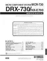
The MCR-730 consists of the DRX-730 and the NX-E700.

 SYSTEM COMPOSITION

DRX-730

NX-E700

Gold color

Black color

Black color
Silver color
White color

White color

Color variations:

Summary of Contents for MCR-730

Page 1: ...s of YAMAHA are continually striving to improve YAMAHA products Modifications are therefore inevitable and specifications are subject to change without notice or obligation to retrofit Should any discrepancy appear to exist please contact the distributor s Service Division WARNING Static discharges can destroy expensive components Discharge any static electricity your body may have accumulated by ...

Page 2: ...y insulated from supply circuits Meter impedance should be equivalent to 1500 ohms shunted by 0 15 μF CAUTION F501 FOR CONTINUED PROTECTION AGAINST RISK OF FIRE REPLACE ONLY WITH SAME TYPE 4A 125V FUSE CAUTION F501 REPLACE WITH SAME TYPE 4A 125V FUSE ATTENTION F501 UTILISER UN FUSIBLE DE RECHANGE DE MÉME TYPE DE 4A 125V All of the P C B s installed in this unit and solder joints are soldered using...

Page 3: ...xposure Laser Emitting conditions 1 When the Top Cover is removed and the STANDBY ON SW is turned to the ON position the laser component will emit a beam for several seconds to detect if a disc is present During this time 5 10 sec the laser may radiate through the lens of the laser pick up unit Do not attempt any servicing during this period If no disc is detected the laser will stop emitting the ...

Page 4: ...ally touch copper tracks and or components when servicing the player Service personnel have to take precautions to prevent touching this area or components in this area Note The screws on the DVD mechanism may never be touched removed or re adjusted Handle the DVD mechanism with care when the unit has to be exchanged The DVD mechanism is very sensitive for dropping or giving shocks Warning for pow...

Page 5: ...micals These can generate electrical charges sufficient to damage ES devices 6 Do not remove a replacement ES device from its protective package until immediately before you are ready to install it Most replacement ES devices are packaged with leads electrically shorted together by conductive foam aluminum foil or comparable conductive material 7 Immediately before removing the protective material...

Page 6: ...by Macrovision Corporation Reverse engineering or disassembly is prohibited Region Management Information This DVD player is designed and manufactured to respond to the Region Management Information that is recorded on a DVD disc If the Region number described on the DVD disc does not correspond to the Region number of this DVD player this DVD player cannot play this disc REGION MANAGEMENT INFORMA...

Page 7: ...7 DRX 730 NX E700 DRX 730 NX E700 Top view FRONT PANELS DRX 730 U C T K A G F L V models NX E700 U C T K A G F L V models ...

Page 8: ...8 DRX 730 NX E700 DRX 730 NX E700 DRX 730 U C models REAR PANELS DRX 730 G model DRX 730 T model DRX 730 F model DRX 730 K model DRX 730 L model DRX 730 A model DRX 730 V model ...

Page 9: ...9 DRX 730 NX E700 DRX 730 NX E700 NX E700 T model U C K A G F L V models T model REMOTE CONTROL PANELS U C K A L V models G F models ...

Page 10: ...e Harmonic Distortion Noise DVD VIDEO CD CD DA REC OUT 0 005 or less Frequency Response PRE OUT CD DA VIDEO CD 10 Hz to 20 kHz DVD 48 kHz sampling 10 Hz to 22 kHz DVD 96 kHz sampling 10 Hz to 44 kHz Video Output Composite 1 Vp p 75 ohms Y Output Component Video Output 1 Vp p 75 ohms Pb Output Component Video Output 0 7 Vp p 75 ohms Pr Output Component Video Output 0 7 Vp p 75 ohms RGB AV MONITOR O...

Page 11: ...ry Speaker cable 4 m x 1 Specifications subject to change without prior notice NX E700 8 5 16 215 8 7 16 175 6 7 8 105 4 1 8 113 4 7 16 271 10 11 16 219 8 5 8 300 11 13 16 15 9 16 14 9 16 255 10 1 16 165 6 1 2 183 7 3 16 DRX 730 NX E700 HDMI the HDMI logo and High Definition Multimedia Interface are trademarks or registered trademarks of HDMI Licensing LLC MPEG Layer 3 audio decoding technology li...

Page 12: ...12 DRX 730 NX E700 DRX 730 NX E700 Top view AM FM TUNER MAIN 2 P C B G F models DVD MODULE P C B SUB 1 P C B MAIN 1 P C B SUB 2 P C B DVD MECHANISM ASS Y 3 5 6 7 1 1 2 3 4 5 6 7 2 4 INTERNAL VIEW ...

Page 13: ...ottom view Front side U C G F V models T K A L models Rear side Serial number SERVICE PRECAUTIONS When DVD MODULE P C B of this unit is replaced the serial number and new ID number device key must be reported to YCJ Yamaha Corporation Japan by email Fig 1 Fig 1 Check the Serial Number The serial number SER NO xxxxxxxx can be found at the bottom of this unit Fig 2 Fig 2 Email ycav keycontrol gmx ya...

Page 14: ... will appear on the TV monitor screen as shown below Note While the ID number device key is displayed never operate any keys of the remote control Fig 4 Fig 5 Check the New ID Number Device key Connection Connect the VIDEO OUT terminal of this unit to the VIDEO IN terminal of the TV monitor with a video pin cable Operation Procedure Perform following steps while watching the TV monitor screen and ...

Page 15: ... cover rearward to remove it Fig 1 2 Removal of Front Panel Unit a Open the disc tray remove the lid and close the disc tray Fig 3 b Remove 2 screws 2 push rivets and then remove 2 side panels Fig 1 c Remove 3 screws Fig 1 d Release 2 hooks pull out the front panel unit forward Fig 1 e Remove CB12 and CB26 Fig 1 3 Removal of DVD Mechanism Ass y and DVD Module P C B a Remove 4 screws and screw Fig ...

Page 16: ...ed in the figure below with a screwdriver until the disc tray is ejected Fig 2 Note An Allen hex socket screwdriver 2 5 mm is recommended for this operation b Gently pull the disc tray out When checking the P C B s Spread the rubber sheet and the cloth Then place this unit on the cloth and check it Fig 3 Reconnect all cables connectors that have been disconnected When connecting the flexible flat ...

Page 17: ...oftware on the PC closed It is also recommended to keep the software on the task tray closed as well Required tools Program downloader program FlashSta exe Firmware DRX730_vx mot DRX730_vx id RS232C cross cable D sub 9 pin female Specifications RS232C conversion jig Part No AAX77610 Confirmation of Firmware Version and Checksum Before and after writing to the microprocessor check the firmware vers...

Page 18: ...own below Fig 1 Fig 1 Operation Procedures 1 Connect the power cable of this unit to the AC outlet 2 While pressing the reset switch of RS232C conversion jig press the STANDBY ON key of this unit to turn on the power Fig 1 3 Start up FlashSta exe the screen will appear as shown below Fig 2 Select Internal flash memory Select the port of RS 232C Fig 2 4 Select the port and data to be transmitted Fi...

Page 19: ...dow 6 Click E P R the screen appears as shown below Fig 4 Click OK to start writing Fig 4 Writing being executed Fig 4 5 Click Refer And select the firmware name Fig 3 The ID code and MCU type are loaded automatically when the file is selected Fig 3 Click OK Fig 3 ...

Page 20: ...agnostic function menu check that the firmware is updated successfully When the displayed firmware version and checksum are different from written ones perform the Writing to the microprocessor procedure all over again 9 End FlashSta exe 10 Disconnect the power cable of this unit from the AC outlet 11 Disconnect the RS232C cross cable RS232C conversion jig and flexible flat cable ...

Page 21: ...NEER Firmware S8CAxxxx BIN Confirmation of Firmware Version Before and after the writing firmware to the module board follow the procedures below to check the firmware version 1 Connect the VIDEO OUT terminal of this unit to the VIDEO IN terminal of the TV monitor with a video pin cable 2 Connect the power cable of this unit to the AC outlet 3 Press the STANDBY ON key of this unit to turn on the p...

Page 22: ...DivX R VOD Off us STEREO Initial Settings Move Select Exit ENTER SETUP Options select ROM version is displayed 7 Move the cursor to Options by pressing the DOWN key on the remote control repeatedly and press the ON SCREEN key Fig 7 The ROM version is displayed Fig 7 8 Press the SETUP key on the remote control to end the SETUP procedure Fig 7 9 Press the STANDBY ON key of this unit to turn off the ...

Page 23: ...k that the firmware version See Confirm of Firmware Version When the displayed firmware version and checksum are different from written ones perform the Writing to the microprocessor procedure all over again Writing is being executed Operation Procedures CAUTION Do not turn off the power while updating the firmware 1 Connect the VIDEO OUT terminal of this unit to the VIDEO IN terminal of the TV mo...

Page 24: ...0kHz 8 AD DATA CHECK 1 PS1 PS2 2 PS3 DC 3 DVD DOCK 4 DEST 5 PANEL KEY 9 PROTECTION HISTORY 1 History 1 2 History 2 3 History 3 4 History 4 5 History 5 6 CLEAR HISTORY 10 POWER OFF FACTOR HISTORY 1 Power OFF factor history 1 2 Power OFF factor history 2 3 Power OFF factor history 3 4 Power OFF factor history 4 5 Power OFF factor history 5 6 CLEAR HISTORY 11 DVD SETTING 1 WRITE ID DVD ID writing 2 C...

Page 25: ... disabled In this mode the SLEEP segment of the FL display of this unit flashes to indicate that the mode is self diagnostic function mode with the protection functions disabled Canceling Self Diagnostic Function Before canceling self diagnostic function execute setting for FACTORY PRESET of main menu No 2 Memory initial ization inhibited or Memory initialized In order to keep the user memory stor...

Page 26: ...ection function has worked its history is stored in memory with a backup Even if no abnormality is noted while servicing the unit an abnormality which has occurred previously can be defined as long as the backup data has been stored The history of the protection function is cleared when self diagnostic function is cancelled by selecting PRESET RESERVED Memory initialized of main menu No 2 or when ...

Page 27: ...Reverse keys of this unit Keys of this unit Functions in Self Diagnostic Function mode In addition to the self diagnostic function menu items functions listed below are available Input selection Muting Power on off Functions related to the tuner and the set menu are not available Initial setting used to start Self Diagnostic Function The following initial setting is used when starting self diagnos...

Page 28: ...ion UC GF LV KA T is displayed PRESET INHIBIT Initialization inhibited RAM initialization is not executed Select this sub menu to protect the values set by the user Note The protection history will not be erased using PRESET INHIBIT CPU TYPE The microprocessor type is displayed PRESET RESERVED Initialization reserved Initialization of the back up IC is reserved Actually initialization is executed ...

Page 29: ...V O L U M E M I N 3 V O L U M E 2 0 d B 3 V O L U M E M A X 3 B A S S T R B L 1 0 3 B A S S T R B L 1 0 3 VOLUME CHECK This menu is used to check the volume level setting VOLUME MIN VOLUME 20dB VOLUME MAX BASS TREBLE 10dB BASS TREBLE 10dB ...

Page 30: ...operation Segment conditions of the FL driver and the FL tube are checked by turning ON and OFF all segments Next the operation of the FL driver is checked by using the dimmer control Then a short between segments next to each other is checked by turning ON and OFF all segments alternately in lattice In the above example the segments in the second row from the top are shorted Checking FL display s...

Page 31: ... is turned off when shorting pins Start the self diagnostic function and select the menu The check result is displayed according to the following display specifications Bluetooth adapter version The firmware version of the YBA 10 YAMAHA connected to the DOCK is displayed DOCK connector OK all Y NG others Check item Short pins Result Display UART loop back test Pins No 14 TX No 18 RX OK Y NG N iPAP...

Page 32: ...K This menu is used to select the MUTE status of HP phones SW 7 D AMP OSC MODE This menu is used to select the operation setting of digital amplifier MUTE The MUTE function of HP phones and SW subwoofer is turned OFF INTERNAL HP MUTE The MUTE function of HP phones is turned ON EXTERNAL 300 kHz SW MUTE The MUTE function of SW subwoofer is turned ON EXTERNAL 350 kHz ...

Page 33: ...alue range the protection function works to turn off the power Reference voltage 5V 500 DV DK DVD DOCK DV DVD power supply detection Normal value 240 or more DK DOCK type detection Reference voltage 5V 255 DESTINATION The destination of this unit is displayed Destination for AD port pin no 97 of IC11 pull up resistance 10k ohms P3 DC Power supply voltage protection detection Power amplifier DC pro...

Page 34: ... V 500 ohm 0 1 2 k 1 2 k 7 9 k 12 7 k 20 7 k V 0 0 2 0 3 0 7 0 8 1 7 1 8 2 7 2 8 3 2 3 3 4 2 4 7 5 0 Value 0 20 30 70 80 170 180 270 280 320 330 420 470 500 pin 89 KEY0 OPEN CLOSE PLAY PAUSE STOP SEARCH SKIP and SEARCH SKIP SEARCH SKIP SEARCH SKIP KEY OFF Key input for AD port Pull up resistance 10 k ohms 9 PROTECTION HISTORY The 5 protection histories are displayed Protection history 1 Protection...

Page 35: ... 1 0 x N O H I S T O R Y 10 POWER OFF FACTOR HISTORY The 5 power OFF factor histories are displayed Power OFF factor history 1 Display Power OFF factor display are as follows Factor Power OFF factor history 2 Power OFF factor history 3 Power OFF factor history 4 Power OFF factor history 5 Power OFF factor history clear Press the OPEN CLOSE key and the power OFF factor history will be initialized M...

Page 36: ... I D I D W r i t e E n t 0 1 D V D C L E A R I D D V D R E W R I T E F W 11 DVD SETTING This mode is prepared mainly for manufacturing use Select DVD CLEAR ID to check the ID number device key of the module board See Check the New ID number for details ...

Page 37: ...P8 29 P28 48 P9 28 P29 47 P10 27 P30 46 P11 26 P31 45 P12 25 P32 44 P13 24 P33 43 P14 23 P34 42 P15 22 P35 21 NC 20 16G 19 15G 18 14G 17 13G 16 12G 15 11G 14 10G 13 9G 12 8G 11 7G P1 10 6G 9 5G 8 4G 7 3G 6 2G 5 1G 4 NP 3 NP 2 NX 1 F1 1G 15G 1 V801 16 BT 133GNK SUB P C B GRID ASSIGNMENT P1 P2 P3 P4 P5 P6 P7 P8 P9 P10 P11 P12 ANODE CONNECTION 1G 15G 1 1 2 1 3 1 4 1 5 1 1 2 2 2 3 2 4 2 5 2 1 3 2 3 1G...

Page 38: ...RT AMP_MODE AMP_CLK AMP_MT AMP_CKSEL SCL_EEP FILAMENT INH_RECA DSDA_EEP iPod_RX iPod_TX 50 49 48 47 46 45 44 43 42 41 40 39 38 37 36 35 34 33 32 31 1 2 3 4 5 6 7 8 9 10 11 12 13 14 15 16 17 18 19 20 21 22 23 24 25 26 27 28 29 30 Timer 16 bit Internal peripheral functions Inputs timer B 6 Three phase motor control circuit Outputs timer A 5 Watchdog timer 15 bits VCC1 ports VCC2 ports A D converter ...

Page 39: ... AMP protection detection OCP H when abnormal L when normal 21 AMP_MODE P81 O D AMP reset H when usual L when resetting 22 AMP_CLK P80 TMR OUT D AMP clock for separate oscillation 300KHz and 350KHz 23 AMP_MT P77 I O D AMP mute control Hiz mute off L mute on 24 AMP_CKSEL P76 O D AMP self oscillation ON OFF H separate oscillation L self oscillation 25 SCL_EEP P75 O EEPROM 12C SCL output for backup P...

Page 40: ...DO P34 O PLL IC serial dataoutput 59 TUCK P33 O PLL IC serial clock output 60 TUDI P32 I PLL IC serial data input 61 TUCE P31 O PLL IC serial CE output 62 VCC2 Power supply 5V 63 P30 I Pulldown 64 VSS GND 65 DA_ZFLG P27 I DAC Zero Flag detection H zero detected 66 DA_LATCH P26 O DAC serial CE output 67 DVDMUTE_EN P25 O DVD MUTE ENABLE output H enable L disable 68 RDS_RST P24 O RDS IC reset output ...

Page 41: ...tion 3 PS3 protect IN 0 to VREF 94 PSPRT2 P102 A D IN Power voltage detection 2 PS2 protect IN 0 to VREF 95 PSPRT1 P101 A D IN Power voltage detection 1 PS1 protect IN 0 to VREF 96 AVSS Connect to VSS GND 97 DEST P100 A D IN AD destination discrimination 0 to VREF 98 VREF A D D A reference voltage input 99 AVCC Connect to VCC terminal 3 3V 100 P97 I Pulldown ohm 0 1 2 k 1 2 k 7 9 k 12 7 k 20 7 k V...

Page 42: ...DIG00 63 53 DIG10 2 data timing clock dot data write scan pulse 17 18 19 20 21 22 23 24 25 26 27 28 29 32 31 30 33 34 35 36 37 38 39 40 41 42 43 44 45 46 47 48 51 49 50 52 53 54 55 56 57 58 59 60 61 62 63 64 1 2 3 4 5 6 7 8 9 10 11 12 13 14 15 16 VP DIG00 DIG01 DIG02 DIG03 SEG12 SEG13 SEG14 SEG15 SEG16 SEG17 SEG18 SEG19 SEG20 SEG21 SEG22 SEG23 SEG24 SEG25 Vcc2 SEG26 RESET CS SCK SDATA Vss XOUT XIN...

Page 43: ...P2 11 SEG32 P3 12 SEG31 P4 13 SEG30 P5 14 SEG29 P6 15 SEG28 P7 16 SEG27 P8 17 SEG26 P9 18 Vcc2 VDD Positive power supply for DIG and SEG outputs 19 SEG25 P10 Segment output Connect to segment anode pins of VFD 20 SEG24 P11 21 SEG23 P12 22 SEG22 P13 23 SEG21 P14 24 SEG20 P15 25 SEG19 P16 26 SEG18 P17 27 SEG17 P18I 28 SEG16 P19 29 SEG15 P20 30 SEG14 P21 31 SEG13 P22 32 SEG12 P23 33 SEG11 P24 34 SEG1...

Page 44: ... 805 FL DISPLAY V801 REMOTE CONTROL U801 L R LPF LPF SPEAKER R SPDIF Optical Out FL DRIVER IC801 INPUT SELECTOR SW808 MAIN VOLUME SW807 STANDBY ON SW806 TS3V340 IC28 G F models U C T K A L V models U C T K A L V models 10 11 21 DVD MECHANISM ASS Y IC8 DOCK 5 6 Lch Volume Tone 27 FM AM TDA8922B IC14 80 81 55 61 77 79 44 45 20 24 29 30 38 40 90 68 71 76 78 I2S L R XL2 3 4 5 18 35 MICROPROCESSOR VIDE...

Page 45: ...P AC IN 20D BD9302FP 6R3V 3R3V VP 5 6V Power Detect Reset 5M 5BU Relay SW501 IC11 12p IC11 19p T502 D513 IC27 IC12 IC15 Q49 Q48 Q47 5SUB 12_RES 7I IGND 20D 15DD 21V IC6 KIA78M05 12FL 12V 12A IC9 IC10 KIA7812API 10T 9A 9B IC5 KIA7809API MAIN See page 53 SCHEMATIC DIAGRAM SUB See page 54 SCHEMATIC DIAGRAM POWER SUPPLY SECTION BLOCK DIAGRAM ...

Page 46: ...LCE FLCK FLDT 12_RES IN COM 5SUB PWR_RY 12_RES FILAMENT 12FL VP 5FL FLG 5M CGND PORTABLE_L PORTABLE_R HPL 15DD 15DD MGND DGND FLG VP 7I IGND HPR 20D 20D AGND AGND 20D 20D PAGND PGND VGND DIGITAL OPTICAL OUT OUT 1 1 3 4 5 7 14 1 4 8 5 8 1 12 24 13 1 4 8 5 1 4 8 5 1 4 8 5 1 31 100 50 80 81 51 30 1 10 20 11 1 14 28 15 1 8 16 9 1 8 16 9 1 3 6 4 1 4 8 5 1 2 5 3 1 8 16 9 OUT IN COM OUT COM IN OUT COM IN...

Page 47: ... Side B MAIN 2 P C B G F models G F models T K A G F L V models U C T K A L V models G F models Ref no Location D2 I5 D6 F3 D8 E6 D11 E4 D17 H3 D19 G2 D20 D4 D21 D4 D28 C4 D35 D3 D37 G4 D38 G2 D39 E4 D40 E4 IC10 E4 IC12 D4 IC15 E4 Q2 G4 Q6 I5 Q22 I3 Q25 F3 Q26 F3 Q27 I3 Q52 I4 Q54 I5 Semiconductor Location ...

Page 48: ...5DD 15DD MGND DGND FGND 21V 7I IGND MAIN 1 CB18 VGND PGND PAGND 20D 20D AGND AGND 20D 20D U C V models T K A G L F models Semiconductor Location Ref no Location D501 H5 D502 G4 D504 F4 D505 F3 D506 F4 D507 F4 D510 D4 D511 D3 D513 C3 D514 E5 D515 E5 D516 D5 IC503 E5 IC506 E5 Q501 G4 Q502 C3 Circuit No U C T K A G L F V L502 O X O J520 523 X O X X NOT USED O USED APPLICABLE ...

Page 49: ...5 6 7 DRX 730 NX E700 49 IC505 IC502 SUB 1 P C B Side B 1 8 16 9 K A R T K A G L F models T K A G L F models Semiconductor Location Ref no Location D503 F4 D508 E3 D509 E3 D512 C3 D517 H3 D518 E5 D519 E5 D521 B3 IC502 F5 IC505 C5 ...

Page 50: ...ON PORTABLE PHONES STOP INPUT VOLUME PLAY PAUSE SUB 2 P C B Side A MAIN 1 CB20 IREA IREB REM VREA VREB ICFL TIMER_LED HDMI_LED PROGRESSIVE STBY HPDET AGND1 AGND1 AGND2 AGND2 KEY0 FLCE FLCK FLDT FILAMENT 12FL VP 5FL FLG 5M CGND PORTABLE_L PORTABLE_R HPL HPR MAIN 1 CB12 USBD USBD 5USB USBG USBG 5USB Semiconductor Location Ref no Location D809 H3 D810 H3 D812 H3 ...

Page 51: ... 3 4 5 6 7 DRX 730 NX E700 51 IC 8 0 1 SUB 2 P C B Side B 1 16 17 49 48 64 32 33 Semiconductor Location Ref no Location D801 D5 D802 D5 D803 D5 D804 D5 D811 C4 IC801 F3 Q801 E3 Q802 H4 Q803 H4 Q804 H3 Q805 C4 Q806 C4 Q807 C4 ...

Page 52: ...1PW TSSOP BA50DD0WHFP BD9302FP E2 BD9778HFP TC74VHC74FT TDA8922BTH Anode Cathode Anode Cathode Anode Cathode Anode Cathode Anode Cathode 1 2 3 A1 A1 K K A2 A2 Anode Cathode MTZJ22D Anode Cathode AC AC ANODE CATHODE D1NL20U 5083 MA8030 3 0V MA8039 H 4 0V MA8051 M 5 1V MA8062 M 6 2V MA8068 M 6 8V MA8100 H 10 3V MA8200 M 20 0V P6KE200ARL S1NB20 1A 200V 1SR154 400 D1FK60 5063 RB051L 40 MAZ8220GHL 1SS3...

Page 53: ...OUT LOUT TRER BASSR1 BASSR2 BASSL2 BASSL1 TREL DGND SDA SCL REFIN AGND VCC Volume Volume Tone control Lch Bass Treble REF IC11 R5F3640DNFA Single chip 16 bit CMOS microprocessor Timer 16 bit Internal peripheral functions Inputs timer B 6 Three phase motor control circuit Outputs timer A 5 Watchdog timer 15 bits VCC1 ports VCC2 ports A D converter 10 bits X 26 channels Clock generation circuit PLL ...

Page 54: ...AGE PROTECTION LATCH SOFT START FAULT MNGT LOW CLAMP DISABLE LEB OSCILATOR 1 10 14 9 15 7 4 5 6 13 12 11 16 HV VREF SS AOMP VFF CS GD 8 3 GIS GND Vcc FMOD OSC MODE SC ZCD AC_OK 3 V 15 uA DRIVER 15 uA 7 7V 1 mA Hiccup mode OCP logic LINE VOLTAGE FEEDFORWARD IC505 NJM431U Adjustable precision shunt regulator ANODE REFERENCE CATHODE 1 2 3 to MAIN 1 _CB18 Page 53 J4 to MAIN 1 _CB21 Page 53 J4 to MAIN ...

Page 55: ... 3 9 0 5 0 16 1 22 3 11 5 4 8 0 0 3 4 9 0 4 9 0 0 PHONES USB PORTABLE INPUT VOLUME SUB 2 52 Display controller Serial receive circuit Digit output circuit Clock generator DIG11 SEG42 51 DIG12 SEG41 50 DIG13 SEG40 49 DIG14 SEG39 48 DIG15 SEG38 47 DIG16 SEG37 46 DIG17 SEG36 45 SEG35 XOUT 6 Vcc1 8 Vcc2 18 Vss 5 Vp 64 XIN 7 CS SCK 3 SDATA 4 RESET 1 SEG00 44 9 SEG34 SEG26 17 19 SEG25 Segment output cir...

Page 56: ...NFRD LED INFRARED MODUL RF MODULATOR RF PHOT CPL PHOTO COUPLER PHOT INTR PHOTO INTERRUPTER PHOT RFLCT PHOTO REFLECTOR PIN TEST PIN TEST POINT PLST RIVET PLASTIC RIVET R ARRAY RESISTOR ARRAY R CAR CARBON RESISTOR R CAR CHP CHIP RESISTOR R CAR FP FLAME PROOF CARBON RESISTOR R FUS FUSABLE RESISTOR R MTL CHP CHIP METAL FILM RESISTOR R MTL FLM METAL FILM RESISTOR R MTL OXD METAL OXIDE FILM RESISTOR R M...

Page 57: ...100 C EL 10uF 25V C70 74 UR866100 C EL 1uF 50V C75 US062100 C CE CHP 100pF 50V B P C B MAIN C76 77 US135100 C CE CHP 0 1uF 16V C78 82 UR866100 C EL 1uF 50V C83 UR847100 C EL 10uF 25V C84 85 UA352220 C MYLAR 220pF 50V C86 87 UR866220 C EL 2 2uF 50V C89 90 US063100 C CE CHP 1000pF 50V B C94 95 UA353220 C MYLAR 2200pF 50V C97 UR838100 C EL 100uF 16V C98 99 UU247100 C EL 10uF 25V C104 US135100 C CE CH...

Page 58: ...P 220pF 50V B C242 UR865470 C EL 0 47uF 50V C243 US135100 C CE CHP 0 1uF 16V C244 UR847100 C EL 10uF 25V C245 WB165500 C EL 0 33F 5 5V C247 US064100 C CE CHP 0 01uF 50V B C249 250 VE326800 C MYLAR 0 47uF 50V C251 UR848100 C EL 100uF 25V C252 253 US065100 C CE CHP 0 1uF 50V B C254 257 US061330 C CE CHP 33pF 50V B C259 US064100 C CE CHP 0 01uF 50V B C263 US064100 C CE CHP 0 01uF 50V B C265 US064100 ...

Page 59: ...1708 S T Q50 VV655700 TR DGT DTC144EKA GF Q51 54 VZ725900 TR 2SD1938F S T R16 HV754100 R CAR FP 10 Ω 1 4W R73 75 VY893200 R MTL OXD 12 Ω 1W R115 WB785000 R MTL OXD 18 Ω 1W J R176 HV754100 R CAR FP 10 Ω 1 4W R180 HV754100 R CAR FP 10 Ω 1 4W R184 HV754100 R CAR FP 10 Ω 1 4W R185 V9199400 R MTL OXD 1 2K Ω 1W R187 HV753220 R CAR FP 2 2 Ω 1 4W R190 HV754100 R CAR FP 10 Ω 1 4W R193 HV753680 R CAR FP 6 8...

Page 60: ...0 DIODE BRG S1NB20 1A 200V D514 WQ545500 DIODE SCHO D5S9M D515 VQ308300 DIODE D1NL40 TP 4083 D516 WQ080900 DIODE SCHO STPS20150CFP 20A D517 VU172800 DIODE ZENR UDZS12B TE 17 12V D518 519 VU998700 DIODE ZENR MA8220 M 22V D521 VT532500 DIODE 1SR154 400 D801 804 VT332900 DIODE 1SS355 D809 810 VU758600 LED gr SLR 342MC D811 VU993400 DIODE ZENR MA8062 M 6 2V D812 VT439400 LED red SLR 342VC3F F501 WG410...

Page 61: ...62 DRX 730 NX E700 A B C D E 1 2 3 4 5 6 7 200 200 1 U C L V models 202 K A G F models 202 203 101 141 141 150 150 105 149 149 141 112 111 141 204 MAIN UNIT FRONT PANEL UNIT OVERALL ASS Y ...

Page 62: ...LAT HEAD B TIGHT SCREW 3x8 MFZN2B3 150 VY712800 PW HEAD B TIGHT SCREW 3x8 8 MFNI33 GD SI WH 150 WE975300 PW HEAD B TIGHT SCREW 3x8 MFZN2B3 BL ACCESSORIES 200 WP507500 REMOTE CONTROL RRS4004 1006EM UCKALV 200 WP507600 REMOTE CONTROL RRS4004 1007EM GF 200 1 AAX57560 BATTERY COVER 103RRS 141 07L 202 V6267000 INDOOR FM ANTENNA 1 4m 1pc UCLV 202 VQ147100 INDOOR FM ANTENNA 1 4m 1pc KAGF 203 VQ307400 AM ...

Page 63: ...64 DRX 730 NX E700 A B C D E 1 2 3 4 5 6 7 1 101 1 103 1 102 1 115 1 111 1 108 1 109 1 110 1 104 1 116 1 116 1 116 1 117 1 117 1 103 1 115 1 12 1 11 FRONT PANEL UNIT ...

Page 64: ...08 WP304500 BUTTON 2P SKIP SEARCH GD 1 108 WP304700 BUTTON 2P SKIP SEARCH BL 1 108 WP304600 BUTTON 2P SKIP SEARCH SI WH 1 109 WP304800 BUTTON STB STANDBY ON GD 1 109 WP305000 BUTTON STB STANDBY ON BL 1 109 WP304900 BUTTON STB STANDBY ON SI WH 1 110 WP305100 BUTTON EJ OPEN CLOSE GD 1 110 WP305300 BUTTON EJ OPEN CLOSE BL 1 110 WP305200 BUTTON EJ OPEN CLOSE SI WH 1 111 WP305400 BUTTON PS PLAY STOP GD...

Page 65: ... 2 121 2 123 2 123 2 121 2 121 2 103 2 103 2 121 2 121 2 124 2 124 2 115 2 121 2 121 2 121 2 6 1 2 121 2 122 2 102 2 124 2 124 2 124 2 124 2 31 2 32 2 22 2 11 2 12 2 36 2 34 2 35 2 33 2 38 2 5 2 6 2 1 2 2 2 1 2 1 1 DVD Mechanism Ass y MAIN UNIT ...

Page 66: ...m A 2 11 WB212300 POWER CABLE 2m GFL 2 11 WC992700 POWER CABLE 2m V 2 12 V2438700 CORD STOPPER 10P1 2 22 WB424000 AM FM TUNER ENG06709Q UCLV 2 22 WB877300 AM FM TUNER FAE381 A07F T 2 22 WB877400 AM FM TUNER FAE481 E07F K 2 22 WB424100 AM FM TUNER ENG07711Q AGF 2 31 WQ277400 FLEXIBLE FLAT CABLE 13P 210mm P 1 0 2 32 WQ277500 FLEXIBLE FLAT CABLE 14P 90mm P 1 0 GF 2 33 WQ277600 FLEXIBLE FLAT CABLE 17P...

Page 67: ...0 FRONT GRILLE ASS Y White color WH 3 XW275B00 DRIVER TWEETER 2 5cm 5 Ω JA05U3 4 XZ668D00 DRIVER WOOFER 11cm 6 Ω JA1151 7 V9504600 NETWORK ASS Y 7 1 V6055400 ELECTROLYTIC CAP 8 2uF 63V C1 7 2 V6367500 ELECTROLYTIC CAP 3 3uF 63V C2 7 3 V9507500 CEMENT RESISTOR 2 7 Ω 5W R1 12 V5361400 TERMINAL CAP S06E RED 13 V5361500 TERMINAL CAP S06E BLACK 21 WE963200 FLAT HEAD WOOD SCREW 3 5x20 MFZN2B3 22 WF82420...

Page 68: ...0 HF45 6300 3 3 kΩ HF45 6330 HF45 6330 3 6 kΩ HJ35 6360 HF85 6360 3 9 kΩ HF45 6390 HF45 6390 4 7 kΩ HF45 6470 HF45 6470 5 1 kΩ HF45 6510 HF45 6510 5 6 kΩ HF45 6560 HF45 6560 6 8 kΩ HF45 6680 HF45 6680 8 2 kΩ HF45 6820 HF45 6820 9 1 kΩ HF45 6910 HF45 6910 10 kΩ HF45 7100 HF45 7100 Value 1 4W Type Part No 1 6W Type Part No 11 kΩ HF45 7110 HF45 7110 12 kΩ HJ35 7120 HF85 7120 13 kΩ HF45 7130 HF45 7130...

Page 69: ...1 32 33 34 35 36 37 38 39 40 41 xx 42 43 44 45 46 47 48 49 KEY No 50 51 19 18 17 16 15 14 13 12 11 Vss E2 E1 XIN XOUT IC1 M34283G2GP W5 U1 Z N0102 86214 1X E0 G0 G1 G2 G3 VDD CARR D0 D1 D2 D3 D4 D5 D6 D7 R2 27 ohms R1 2 ohms 1 4W Q1 2SC3440 T112 C2 Not mount X1 T1 4MHz C1 47μF 3 0V REMOTE CONTROL PANEL SCHEMATIC DIAGRAM U C K A L V models G F models ...

Page 70: ...M 7C D7 14 ON SCREEN 7C A6 15 AUDIO 7C AD 16 SUBTITLE 7C AA 17 ANGLE 7C AE 18 PLAY MODE 7C BD 19 7C 85 20 CLEAR 7C 9F 21 7C 86 22 7C 83 23 7C 87 24 7C B9 25 7C 82 26 7C BA Key No Label English Custom Code Data Code Upper Case 27 TOP MENU INFO 7C B1 28 78 8E 29 MENU 7C B2 30 78 9F 31 ENTER 78 C1 32 78 9E 33 SET UP 7C AC 34 78 8F 35 RETURN 7C B7 36 AUTO MANUAL 78 B7 37 MEMORY 78 B2 38 VOLUME 78 1E 3...

Page 71: ...DRX 730 NX E700 ...

Reviews: