background image

3 - 5

2. SERVO BLOCK DIAGRAM

3 - 6

Summary of Contents for DVD-S795

Page 1: ...MAHA Retailer or the appointed service representaive IMPORTANT The presentation or sale of this manual to any individual or firm dose not constitute authorization certification or recognition of any a...

Page 2: ...2 15 17 Disassembling the Pulley Gear and Deceleration Gear 2 15 18 Disassembling the Mechanism Loading C B A 2 15 19 Lubricating the Optical Pickup and Peripheral parts 2 16 ELECTRICAL ADJUSTMENT 1...

Page 3: ...Pin jack Audio output Output level 2 Vrms 1kHz 0dB Output connector Pin jack 5 1ch mixed output 1 system 2ch 5 1ch discrete output 1 system 5 1ch Audio signal output characteristics 1 Frequency respo...

Page 4: ...TECTION OF EYES FROM LASER BEAM DURING SERVICING This set employs a laser Therefore be sure to carefully follow the instructions below when servicing 1 Pick up Wave length 655nm Laser power CLASS II 2...

Page 5: ...e electrical charge sufficient to damage ES devices 5 Do not use freon propelled chemicals These can generate electrical charges sufficient to damage ES devices 6 Do not remove a replacement ES device...

Page 6: ...kup 1 Do not subject the optical pickup to static electricity as it is extremely sensitive to electrical shock 2 To prevent the breakdown of the laser diode an antistatic shorting pin is inserted into...

Page 7: ...DVD S795 S705 1 5 REAR PANELS U C models DVD S795 S705 B G models G model Gold A model...

Page 8: ...into the unit if it is 40 or less Check the laser drive current Value is more than 50 Value is 50 or less Initialize the player Press Pause and and Open Close buttons on unit simultaneously End Refer...

Page 9: ...to Initializing the DVD Player in page 1 9 0 5 7 6 9 1 Service Mode Table The service mode can be activated by pressing various button combinations on the player and remote control unit 2 Self Diagnos...

Page 10: ...cuit IC6201 IC6201 IC6201 IC6201 IC6201 IC6201 IC6201 IC6302 IC6303 4 Sales Demonstration Lock Function This function prevents discs from being lost when the unit is used for sales demonstrations by d...

Page 11: ...and Equipment Table DVDT S15 AX07320 or DVDT S01 TX946080 JZS0100 TX946380 JGS0099 TX946360 JGS0098 TX946370 2 RZZ0L01 TX946400 JGS0091 TX946260 JGS0092 TX946270 JZS0648 TX946410 JGS0101 TX946390 SZZ...

Page 12: ...mplifier containing Dolby Digital or dts digital theater systems decoder When DVDs recorded in Dolby Digital or dts are played Dolby Digital bitstream or dts bitstream is output from the player s OPTI...

Page 13: ...etting see page 40 the discs recorded in Linear PCM will be played back only in 2 channels even when the center speaker is connected as well as the front speakers DVDs recorded in Linear PCM 96 kHz sa...

Page 14: ...For some functions the setting will be registered imme diately for others SELECT or PLAY must be pressed When numbers are displayed e g title No the numeric buttons are also effective for setting ins...

Page 15: ...V2 V1 V2 Change the No by using the cursor buttons or the numeric buttons ENG English POR Portuguese FRA French RUS Russian DEU German JPN Japanese ITA Italian CHI Chinese ESP Spanish KOR Korean NLD D...

Page 16: ...laying time Remaining time of the track Remaining time of the disc Audio mode Video CD only Change the mode by using the cursor buttons LR L R Left channel sound is output from the speaker L and right...

Page 17: ...clear a marker select the preferred marker no using the cursor buttons and press CLEAR Adjust the master volume by using the cursor buttons 0 to 127 dB or Master volume Contrast 7 to 7 Equalizer 1 0...

Page 18: ...aximum speeds of rapid reverse and rapid advance DVD 100 100 Video CD 40 40 CD 50 50 Detailed descriptions of each On Screen Menu Icon Shuttle screen Still Pause Press the cursor button Slow motion pl...

Page 19: ...sembly Procedure When servicing the unit use the following procedure to disassemble the casing and inside parts for internal inspection Tray Front panel Rear panel Power Supply C B A V Comp C B A U C...

Page 20: ...Casing Parts and C B A Positions 3 Service Positions Note To inspect the loading base unit position the left side upward as viewed from the front Module C B A Power supply C B A TX946370 TX946370 TX9...

Page 21: ...and right 3 Release the 2 tabs 4 Disconnect the 2 flexible cables Tab Flexible cable Flexible cable 5 Disassembling the Tray 1 Turn the level clockwise 2 Move the tray in the direction of the arrow un...

Page 22: ...s varies according to the model Screw Screw Screw Screw 2 Release the two tabs on the left and right 2 Connect the module C B A to the mother C B A with the extension cables for inspection Extension c...

Page 23: ...on cable TX946360 JGS0099 connects the power supply C B A PS1101 and the mother C B A PP1101 3 Checked by connecting the module C B A and the mother C B A with the extension cables Extension cables TB...

Page 24: ...kup 3 Testers cannot be used to check the laser diode of the optical pickup The power supply inside the tester can easily damage the laser diode 4 Take care when handling the flexible cable because ex...

Page 25: ...01g Grease EM 30LG TX946270 0 01g Grease EM 30LG TX946270 0 01g Grease EM 30LG TX946270 0 01g Grease EM 30LG TX946270 0 02g Grease EM 30LG TX946270 0 02g Grease EM 30LG TX946270 0 01g Intermediate cha...

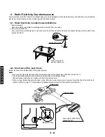
Page 26: ...ntermeasure Methods Solder the land in the flexible cable of the optical pickup Notes Be sure to do this befer disconnecting the flexible cable of the optical pickup from the module C B A Use an anti...

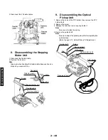
Page 27: ...Note Be sure to take static electricity counterneasures before disconnecting the flexible cable Refer to page 2 8 Static Electricity Countermeasures 1 Remove the tab and pull out the clamper 7 Disass...

Page 28: ...st the optical pickup titl after replacing the optical pickup Refer to page 2 13 Optical Pickup Tilt Adjustment 8 Disassembling the Stepping Motor Unit 1 Disconnect the flexible cable 2 Remove the 2 s...

Page 29: ...ore replacing the optical pickup remove the sub shaft preload spring for use with the new optical pickup After installation use screw lock to lock the screw in position 12 Assembling the Optical Picku...

Page 30: ...optical pickup tilt after replacing the spindle motor unit 4 Remove the solder from the pickup FPC s soldered short circuit 5 Adjust the optical pickup tilt after removing the solder Refer to page 2 1...

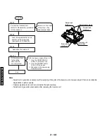
Page 31: ...STEP4 STEP5 STEP6 NG OK STOP PAUSE button main unit OPEN CLOSE button main unit 5 button remote control unit Press simultaneously Main unit display Check to see that JIT xxx is displayed Present jitt...

Page 32: ...n to turn off the power 3 Disconnect the power plug from the outlet Assemble the main unit Follow procedure for handling after repairs are completed End STEP6 Adjustment screws Screw lock 0 02 g Screw...

Page 33: ...embling the Intermediate Chassis 1 Push the stopper downward then rotate it until it contacts the vertical cam 2 Release the 2 tabs 18 Disassembling the Mechanism Loading C B A 1 Remove the 2 screw 2...

Page 34: ...946P part number TX946410 0 01g Screw lock Three Bond 1401C 0 02g part number TX946400 Screw lock Three Bond 1401C 0 02g part number TX946400 Screw lock Three Bond 1401C 0 02g part number TX946400 MC...

Page 35: ...terminate at 75 ohms 2 Adjust VR3501 so that the luminance signal Y S level becomes 1000 mVp p 20 mV 2 Video Output Chrominance Signal Adjustment Do this adjustment after replacing a C B A Measurement...

Page 36: ...value Screwdriver Oscilloscope 100mV div 10 sc div 525mVp p 11mV B A G Models 486mVp p 10mV U C Models DVDT S15 AX07320 or DVDT S01 TX946080 Purpose To maintain video signal output compatibility 1 Con...

Page 37: ...SE WAVE MOTOR DRIVE A PWMOA B PULSE WAVE MOTOR OUT A B INITIAL LOGO ABBREVIATIONS SECTION3 ABBREVIATIONS A A0 UP ADDRESS ACLK AUDIO CLOCK AD0 UP ADDRESS BUS ADATA AUDIO PES PACKET DATA ALE ADDRESS LAT...

Page 38: ...A SYSCLK SYSTEM CLOCK T TE TRACKING ERROR TIBAL BALANCE CONTROL TID BALANCE OUTPUT 1 TIN BALANCE INPUT TIP BALANCE INPUT TIS BALANCE OUTPUT 2 TPSN OP AMP INPUT TPSO OP AMP OUTPUT TPSP OP AMP INVERTED...

Page 39: ...3 3 3 4 BLOCK DIAGRAM 1 OVERALL BLOCK DIAGRAM...

Page 40: ...3 5 2 SERVO BLOCK DIAGRAM 3 6...

Page 41: ...3 7 3 VIDEO BLOCK DIAGRAM 3 8...

Page 42: ...3 9 4 AUDIO BLOCK DIAGRAM 3 10...

Page 43: ...3 11 SCHEMATIC DIAGRAM 1 POWER SUPPLY SCHEMATIC DIAGRAM FOR U C MODELS 5 1 5 1 0 0 0 3 4 3 3 5 1 3 4 0 12 5 3 4 8 9 8 9 0 5 2 4 1 16 6 0 5 3 9 2 5 0 0 5 0 2 17 0 26 0 0 0 0 U C MODELS 3 12...

Page 44: ...8 9 8 9 0 0 0 0 0 12 5 3 4 3 4 3 4 3 3 5 1 5 1 5 1 5 2 16 6 0 5 4 1 3 9 2 5 0 0 5 0 2 17 0 0 0 0 26 0 3 13 2 POWER SUPPLY SCHEMATIC DIAGRAM FOR B G A MODELS 3 14 B G A MODELS...

Page 45: ...8 79 80 STOP 0 0 1 4 0 0 0 PLAY 0 1 0 5 0 1 2 1 3 1 0 1 95 96 97 98 99 100 STOP 0 0 3 1 0 1 0 1 1 6 PLAY 1 2 0 3 1 1 5 1 9 1 6 101 102 103 104 105 106 107 108 109 110 111 112 113 114 115 116 117 118 1...

Page 46: ...6 2 2 0 3 2 2 0 0 0 0 0 5 0 0 8 2 2 2 9 0 3 5 2 1 2 1 5 0 4 9 0 2 3 1 0 3 5 0 3 1 0 0 0 2 3 1 8 9 8 8 8 9 8 8 1 4 1 4 1 4 1 4 1 4 1 2 1 4 1 2 0 0 2 4 3 1 2 3 1 2 5 8 3 2 5 8 3 2 2 2 5 1 0 1 1 4 1 4 0...

Page 47: ...9 70 71 72 73 74 75 76 77 78 79 80 STOP 3 1 3 0 3 1 0 0 1 5 0 0 3 1 0 3 1 0 0 3 1 1 4 0 0 0 0 3 1 PLAY 3 1 2 8 3 1 1 5 1 5 1 5 3 1 0 3 1 1 4 3 1 0 1 4 3 1 0 1 5 0 0 0 3 1 81 82 83 84 85 86 87 88 89 90...

Page 48: ...3 3 4 9 1 6 1 1 2 4 4 8 4 7 2 4 0 0 0 2 2 1 8 0 1 4 9 2 8 2 6 0 0 0 1 2 4 0 6 2 2 0 0 1 0 3 2 2 0 0 6 0 3 3 0 0 0 0 0 2 3 1 3 1 4 0 8 0 7 5 0 4 9 5 0 4 9 3 3 0 0 2 0 0 2 0 0 2 0 0 1 1 7 0 1 0 0 8 0 3...

Page 49: ...43 44 45 46 47 48 49 50 51 52 53 54 55 56 57 58 59 60 STOP 0 0 0 4 9 0 0 0 1 0 1 1 6 0 1 3 1 0 4 9 0 4 9 0 0 2 2 2 5 0 PLAY 0 3 0 2 2 4 4 9 0 0 0 1 0 2 0 1 1 5 3 1 0 3 4 8 0 4 8 0 5 1 2 2 2 2 0 2 0 61...

Page 50: ...39 40 STOP 3 1 3 1 1 4 3 1 0 2 5 2 5 2 5 2 3 0 2 2 2 3 0 3 1 2 1 2 8 2 8 2 8 2 0 2 0 PLAY 0 0 1 4 3 1 3 1 1 8 2 0 2 2 0 0 0 6 0 3 0 3 3 1 0 0 0 0 0 0 41 42 43 44 45 46 47 48 49 50 51 52 53 54 55 56 5...

Page 51: ...1 4 1 5 1 4 1 4 1 4 1 4 1 4 1 4 1 3 2 3 1 3 2 3 1 3 1 4 1 3 1 5 1 4 1 3 1 4 2 4 1 4 0 0 0 1 5 1 5 1 5 3 1 3 1 1 5 3 2 3 2 0 1 2 0 1 4 0 1 2 0 1 2 0 1 2 1 5 1 2 0 0 0 0 4 9 0 1 2 4 9 0 3 3 2 4 3 0 3 1...

Page 52: ...0 2 1 8 1 9 1 9 2 0 0 0 2 3 1 3 1 2 7 61 62 63 64 65 66 67 68 69 70 71 72 73 74 75 76 77 78 79 80 STOP 3 1 3 1 0 4 0 0 3 1 0 3 1 0 3 1 0 3 1 3 1 3 1 0 1 3 1 0 0 1 0 0 2 PLAY 3 1 2 6 2 6 4 0 0 3 3 1 0...

Page 53: ...0 0 0 0 4 9 0 1 7 1 9 1 7 1 9 1 7 1 9 0 0 2 2 3 1 3 1 3 1 2 2 2 5 1 1 1 3 1 0 1 2 4 9 4 9 1 8 3 2 1 0 1 3 1 3 2 0 1 5 3 1 1 2 2 3 2 4 2 0 2 4 2 0 2 4 2 0 2 4 2 4 1 5 1 6 3 1 0 2 5 2 5 0 0 0 0 0 0 0 0...

Page 54: ...8 4 8 0 1 0 2 5 0 0 0 0 0 0 0 0 1 5 0 5 0 5 0 5 0 2 9 0 5 0 0 5 0 0 5 0 0 0 0 2 5 0 2 4 2 4 4 8 5 0 5 0 4 8 4 8 4 8 4 8 4 8 0 1 4 8 5 0 5 0 5 0 4 8 4 8 4 8 0 4 8 4 8 2 4 2 4 5 0 0 1 1 6 0 1 5 1 4 4 8...

Page 55: ...8 5 8 4 8 4 9 0 9 0 9 0 9 0 0 9 0 9 0 9 0 8 0 2 0 2 0 2 0 2 0 0 0 0 0 0 0 0 0 0 0 0 0 0 0 0 0 0 0 0 0 0 0 0 0 0 0 0 0 0 0 0 0 0 0 0 0 0 0 0 0 0 9 0 9 0 0 0 0 0 0 0 0 5 0 0 2 0 2 0 2 0 2 8 9 5 0 9 0 9...

Page 56: ...9 0 7 4 9 0 0 0 0 7 4 9 0 7 4 9 0 0 0 0 7 4 9 0 7 4 9 0 0 0 0 7 4 9 0 7 4 9 0 0 0 2 4 2 4 2 5 2 5 5 0 0 2 4 2 5 2 5 5 0 0 0 0 0 0 0 0 9 0 8 9 9 0 8 5 8 9 8 8 8 9 8 4 9 0 9 0 9 0 8 3 0 0 7 9 5 8 8 9 5...

Page 57: ...8 8 28 8 28 8 28 8 28 8 28 7 21 4 PLAY 17 5 14 5 21 8 2 8 2 9 14 5 2 8 24 3 26 6 2 8 2 9 3 0 27 0 27 0 26 9 2 9 26 9 26 9 2 9 19 8 41 42 43 44 45 46 47 48 49 50 51 52 53 54 55 56 57 58 59 60 STOP 21 8...

Page 58: ...0 0 0 0 9 0 0 9 0 4 9 2 7 2 6 2 7 2 6 3 41 16 VIDEO COMP SCHEMATIC DIAGRAM FOR U C MODELS U C MODELS 3 42...

Page 59: ...0 7 0 5 13 1 13 3 5 0 0 0 0 2 5 11 1 11 7 11 1 13 1 13 4 0 1 0 1 0 1 0 1 2 1 2 4 2 1 2 3 2 1 2 6 2 1 2 5 2 1 2 5 2 1 2 5 5 1 5 1 0 7 0 7 0 0 7 2 8 2 8 0 2 8 0 3 3 3 3 8 5 1 0 0 0 0 0 0 0 0 0 0 0 0 0...

Page 60: ...9 0 0 0 0 0 8 9 0 0 3 45 18 FRONT SW HEAD PHONE POWER SW SCHEMATIC DIAGRAM 3 46...

Page 61: ...1022 R1032 R1056 R1055 R1031 R1021 D1022 C1019 C1011 D1001 C1021 LB1021 C1010 3 2 4 1 D1011 C1003 1 2 4 3 3 4 2 1 L1001 C1008 C1005 D1002 DZ1001 F1001 T1021 P1001 L1002 1 2 HOT COLD W001 W003 W002 W15...

Page 62: ...022 R1032 R1056 R1055 R1031 R1021 D1022 C1018 C1011 D1001 C1021 LB1021 C1010 3 2 4 1 D1011 R1002 C1003 1 2 4 3 3 4 2 1 L1001 C1008 C1005 F1001 T1021 P1001 L1002 1 2 HOT COLD W001 W003 W002 W154 W102 W...

Page 63: ...E B Q3303 C E B Q3301 C E B IC3281 1 D3301 2 1 2 C E B 4 5 1 8 2 IC3322 3 1 4 5 Q3322 C E B Q3321 C2506 R2502 C2508 R2511 R2520 R2521 C2504 C2512 C2511 C2510 C2509 R2515 C2503 C E B Q3305 C E B C6604...

Page 64: ...004 R3037 R3038 IC3061 C3039 C3036 C3063 C3062 C3035 C3061 C3051 C3066 C3052 C3053 C3065 C3054 R3010 C3045 C3006 C3007 C3008 C3009 C3010 C3011 C3259 R3253 R3252 NJ3201 C3256 LB2521 LB5211 FP5201 LB251...

Page 65: ...592 R4599 D4597 R4597 R4596 R4594 R4591 D4595 D6004 D6003 D6002 R6023 R6022 1 3 5 4 1 3 5 4 IC6005 IC6004 54 53 50 45 40 36 17 15 10 5 2 1 3 2 1 DL6001 IC6003 K4241 LB4241 C4279 C3609 C3532 L3531 R361...

Page 66: ...1 9 8 R4731 L4732 R4736 R4721 R4724 R4723 R4737 R4738 R4722 R4735 R4732 R4733 R4734 C4733 C4731 C4735 C4734 C4736 C4738 C4737 C4732 L4733 L4731 JA 1 3 C4739 C B E C B E REF NO 20000 SERIES A B 1 2 POW...

Page 67: ...51 4 1 2 2 10 20 1 9 21 10 20 1 9 21 5 8 L3882 L3872 L3871 LB3872 LB3873 LB3874 IC3812 16 12 9 1 5 8 D3863 1 2 5 3 Q3852 1 2 6 3 C B E C B E C B E QR3852 1 2 5 3 C B E Q3864 C B E 1 3 6 4 Q3861 C B E...

Page 68: ...ZENER DIODE DIODE ZENR ZENER DIODE DSCR CE CERAMIC DISCRIMINATOR FER BEAD FERRITE BEADS FER CORE FERRITE CORE FET CHP CHIP FET FL DSPLY FLUORESCENT DISPLAY FLTR CE CERAMIC FILTER FLTR COMB COMB FILTE...

Page 69: ...51 C1143 FX612760 C 33uF 25V VCEA1EJC330 C1151 AAX05290 C EL 270uF 25V UC VCEA1EJH271 C1151 FX611840 C EL 390uF 25V ABG EEUFA1E391 C1153 FX612750 C 220uF 25V VCEA1EJC221 C1154 AAX05280 C EL 220uF 16V...

Page 70: ...UX1H220JCV C3051 FX612220 C CE 0 1uF 16V CH ECUX1C104ZFV C3052 FX612220 C CE 0 1uF 16V CH ECUX1C104ZFV C3053 FX612220 C CE 0 1uF 16V CH ECUX1C104ZFV C3054 FX612220 C CE 0 1uF 16V CH ECUX1C104ZFV C3055...

Page 71: ...612090 C CE 0 1uF 50V CH BG ECUM1H104ZFN C3813 FX612090 C CE 0 1uF 50V CH BG ECUM1H104ZFN C3814 FX612090 C CE 0 1uF 50V CH BG ECUM1H104ZFN C3815 FX612090 C CE 0 1uF 50V CH BG ECUM1H104ZFN C3816 FX6120...

Page 72: ...E 0 1uF 50V CH ECUM1H104ZFN C4394 FX612090 C CE 0 1uF 50V CH ECUM1H104ZFN C4395 FX611520 C EL 10uF 16V ECA1CAK100X C4396 FX611550 C EL 47uF 16V ECA1CAK470X C4397 FX611530 C EL 100uF 16V ECA1CAK101X C4...

Page 73: ...5234 FX611880 C EL 33uF 6 3V EEVHB0J330 C5235 NX702420 C CE 3 3uF 10V ECUM1A335KBM C5236 FX612210 C CE 0 1uF 16V CH ECUX1C104KBV C5237 FX612300 C CE 1000pF 50V CH ECUX1H102KBV C5238 NX702470 C CE 0 22...

Page 74: ...A7300B D1041 AAX05690 DIODE MA165 UC MA165 D1041 iX637030 DIODE MA165VT ABG MA165VT D1042 AAX05690 DIODE MA165 UC MA165 D1051 iX637380 DIODE MA700 MA700 D1052 iX637370 DIODE MA4200 H MA4200H D1111 NX7...

Page 75: ...3460 IC M5218AFP M5218AFP IC4751 NX701830 IC TC7W04F TC7W04F IC4781 NX701790 IC T0TX178 T0TX178 IC4901 AAX03550 IC PQ09DZ1U PQ09DZ1U IC5201 AAX05020 IC RN5RZ20BATR RN5RZ20BATR IC5202 AAX03420 IC AN870...

Page 76: ...L 22uH VLQEL05S220J L5201 GX609480 COIL 10uH VLQ0779K100 L5202 GX609480 COIL 10uH VLQ0779K100 L6001 AAX05360 COIL 100uH VLQEL05S101J L6002 AAX05370 COIL 220uH VLQEL05S221J L6005 AAX05360 COIL 100uH VL...

Page 77: ...LB6016 AAX03840 COIL VLP0153 LB6213 GX609450 COIL VLP0155 LB6521 AAX05730 COIL CHP VLP0323A601R LB6522 GX609460 COIL VLP0157 LB6523 AAX05730 COIL CHP VLP0323A601R LB6525 GX609460 COIL VLP0157 LB6526 G...

Page 78: ...853 AAX05760 TR DGT XN1112 BG XN1112 QR3861 AAX05750 TR DGT UN2217 BG UN2217 QR3862 AAX05770 TR DGT XN1213 BG XN1213 QR3863 AAX05770 TR DGT XN1213 BG XN1213 QR4591 NX702780 TR DGT UN2211 UN2211 QR4592...

Page 79: ...W ERJ3GEYJ392 R3005 HX610010 R MTL CHP 10K 1 16W ERJ3GEYJ103 R3006 HX610190 R MTL CHP 47K 1 16W ERJ3GEYJ473 R3008 HX610190 R MTL CHP 47K 1 16W ERJ3GEYJ473 R3009 HX610100 R MTL CHP 220 1 16W ERJ3GEYJ22...

Page 80: ...65 AAX07060 R MTL CHP 330 1 10W UCBG ERJ6GMYJ331 R3571 AAX07120 R MTL CHP 560 1 10W UCBG ERJ6GMYJ561 R3572 AAX06990 R MTL CHP 18K 1 10W UCBG ERJ6GMYJ183 R3573 AAX07090 R MTL CHP 470 1 10W UCBG ERJ6GMY...

Page 81: ...0 R MTL CHP 750 1 10W ERJ6GMYJ751 R4332 AAX07150 R MTL CHP 750 1 10W ERJ6GMYJ751 R4333 AAX06950 R MTL CHP 1K 1 10W ERJ6GMYJ102 R4341 AAX06940 R MTL CHP 100 1 10W ERJ6GMYJ101 R4342 AAX06970 R MTL CHP 1...

Page 82: ...GMYJ220 R4771 AAX07140 R MTL CHP 75 1 10W ERJ6GMYJ750 R4901 AAX07190 R MTL CHP 8 2K 1 10W ERJ6RBD822 R4902 AAX07180 R MTL CHP 1 5K 1 10W ERJ6RBD152 R4903 AAX07070 R MTL CHP 33K 1 10W ERJ6GMYJ333 R4911...

Page 83: ...6330 VR TRIM EVNCYAA03B13 VR3511 AAX06330 VR TRIM EVNCYAA03B13 VR4721 AAX06200 VR EVJCAEF01A14 W077 AAX04160 DIODE AK04WS AK04WS W101 HX610350 R MTL CHP 0 1 10W ERJ6GEY0R00 W102 HX610350 R MTL CHP 0 1...

Page 84: ...ASS Y MOTHER VEP99133N A 9 AAX03340 CODE 9P VWJ1299 10 AAX06160 REAR PANEL DVD S795 VMA0B53 10 AAX06170 REAR PANEL DVD S705 VMA0B54 10 AAX06180 REAR PANEL VMA0B55 10 AAX06190 REAR PANEL VMA0B56 11 AA...

Page 85: ...HD0690 B 5 AAX04420 SCREW XYE3 EF12 B 6 AAX04430 SCREW XYE3 EF20 B 7 AAX04440 SCREW XYE3 EF25 B 8 AAX04370 SCREW VHD1258 B 9 EX604040 SCREW XTV3 10G B12 EX604040 SCREW XTV3 10G ACCESSORIES 108 NX70313...

Page 86: ...3 4 5 6 7 3 Loading Mechanism Section 3 1 Loading Mechanism Section Exploded View 4 21 B43 B44 B42 B42 48 E LOADING MOTOR C B A TO MODULE C B A 50 41 42 44 55 43 47 52 54 51 53 45 B45 B45 B46 B41 B41...

Page 87: ...47 CX680240 BELT VDV0373 48 AAX01240 P C B ASS Y MECH LOADING VEP90407A 49 AAX04580 BASE LOADING VMD3266 50 AAX03790 CLAMP BASE VMD3263 51 AAX04650 MAGNET JSM0048 52 CX680160 CLAMPER BACK YOKE VMA953...

Page 88: ...7 4 Traverse Section 4 1 Traverse Section Exploded View 4 23 63 74 72 61 B61 B61 B64 B63 B61 B61 B61 B62 B65 B65 B65 B62 B62 70 69 76 68 65 69 66 73 75 62 64 64 69 71 67 TO SPINDLE MOTOR TO MODULE C...

Page 89: ...ATING RUBBER VMG1166 70 AAX04260 TRAVERSE CHASSIS VMK0474 71 AAX03750 GUIDE SHAFT 1 VMS6471 72 AAX03760 GUIDE SHAFT 2 VMS6472 73 AAX03180 OPTICAL PICKUP HEAD VED0402 74 AAX04780 SPRING VMC1491 75 AAX0...

Page 90: ...19 18 17 16 15 14 13 12 11 PD64GS430T1 00 33 AUDIO 2 CUSTOM CODE DATA CODE FUNCTION Key No 00 0A PLAY 3 00 87 7 00 00 STOP 8 00 8E MARKER 10 00 05 SLOW SERCH 11 00 11 2 12 00 94 SET UP 14 00 4A SKIP...

Reviews: