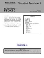
HF/50 MHz TRANSCEIVER
FTDX10
Introduction
This manual provides the technical information necessary
for servicing the FTDX10 HF/50 MHz TRANSCEIVER.
Servicing this equipment requires expertise in handling
surface-mount chip components. Attempts by non-qualified
persons to service this equipment may result in permanent
damage not covered by the warranty, and may be illegal in
some countries.
While we believe the information in this manual to be cor-
rect, YAESU assumes no liability for damage that may oc-
cur as a result of typographical or other errors that may be
present. Your cooperation in pointing out any inconsisten-
cies in the technical information would be appreciated.
Important Note
This transceiver was assembled using Pb (lead) free solder, based on the RoHS specification.
Only lead-free solder (Alloy Composition: Sn-3.0Ag-0.5Cu) should be used for repairs performed on this apparatus. The solder stated
above utilizes the alloy composition required for compliance with the lead-free specification, and any solder with the above alloy com
-
position may be used.
Technical Supplement
EH076H90A
©2021 YAESU MUSEN CO., LTD.
Contents
Exploded View
Block Diagram
Connection Diagram
Alignment
Board Unit (Schematics, Layouts & Parts)
MAIN Unit
FINAL Unit
DISPLAY Unit
SW Unit
MEMORY Unit
VR Unit
ENC-A Unit
ENC-B Unit
DC-DC Unit
Summary of Contents for FTDX10
Page 8: ...BLOCK DIAGRAM 1 FTDX10 Technical Supplement Block Diagram...
Page 9: ...CONNECTION DIAGRAM 1 FTDX10 Technical Supplement Connection Diagram...
Page 29: ...FTDX10 Technical Supplement MAIN 1 MAIN Unit Circuit Diagram MAIN Unit CNTL...
Page 30: ...FTDX10 Technical Supplement MAIN 2 MAIN Unit Circuit Diagram MAIN Unit DVI...
Page 31: ...FTDX10 Technical Supplement MAIN 3 MAIN Unit Circuit Diagram MAIN Unit DSP...
Page 32: ...FTDX10 Technical Supplement MAIN 4 MAIN Unit Circuit Diagram MAIN Unit AF...
Page 33: ...FTDX10 Technical Supplement MAIN 5 MAIN Unit Circuit Diagram MAIN Unit RX...
Page 34: ...FTDX10 Technical Supplement MAIN 6 MAIN Unit Parts Layout side A 1 2 3 4 5 6 7 A B C D E F G H...
Page 35: ...FTDX10 Technical Supplement MAIN 7 MAIN Unit Parts Layout side B 1 2 3 4 5 6 7 a b c d e f g h...
Page 74: ...FTDX10 Technical Supplement FINAL 1 FINAL Unit Circuit Diagram...
Page 91: ...FTDX10 Technical Supplement DISPLAY 1 DISPLAY Unit Circuit Diagram...
Page 92: ...FTDX10 Technical Supplement DISPLAY 2 DISPLAY Unit Parts Layout side A 1 2 3 4 A B C D E F G...
Page 93: ...FTDX10 Technical Supplement DISPLAY 3 DISPLAY Unit Parts Layout side B 1 2 3 4 a b c d e f g...
Page 103: ...FTDX10 Technical Supplement SW 1 SW Unit Circuit Diagram...
Page 104: ...FTDX10 Technical Supplement SW 2 SW Unit Parts Layout side A 1 2 3 4 A B C D E F...
Page 105: ...FTDX10 Technical Supplement SW 3 SW Unit Parts Layout side B 1 2 3 4 A B C D E F...
Page 108: ...MEMORY 1 Circuit Diagram FTDX10 Technical Supplement MEMORY Unit...
Page 109: ...MEMORY 2 Parts Layout side A FTDX10 Technical Supplement MEMORY Unit...
Page 110: ...MEMORY 3 Parts Layout side B FTDX10 Technical Supplement MEMORY Unit...
Page 113: ...ENC A 1 Circuit Diagram side A side B Parts Layout FTDX10 Technical Supplement ENC A Unit...
Page 116: ...FTDX10 Technical Supplement DC DC 1 DC DC Unit Circuit Diagram...
Page 117: ...FTDX10 Technical Supplement DC DC 2 DC DC Unit Parts Layout side A side B...


