7
Alignment
m
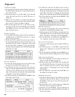
Tune the transceiver to the 144.5000 MHz, and select
the USB mode.
m
Key the transmitter, and adjust VR3501 for 1.5 ~ 1.6 A
on the ammeter.
m
Disconnect the ammeter, and reinstall the jumper con-
nector at J3502.
VHF/UHF Final Idling Current Adjustment
m
Leave the coaxial plug disconnected from J3501, and
be sure that the 50-
W
resistor is connected across its
socket. Connect the ammeter between the transceiver’s
13.8VDC connector and the DC power supply.
m
Tune the transceiver to 144.5000 MHz, and select the
USB mode.
m
Key the transmitter, and adjust VR3502 for 2.3 A ±0.1 A
on the ammeter.
m
Disconnect the ammeter, and reinstall the jumper con-
nector at J3501.
TX and RX IF Adjustments
HF Band RX IF Sensitivity (Coarse Adjust)
m
Preset “Alignment” Menu items F-03 [HF RX IF G], F-
04 [50 RX IF G], F-05 [144 RX IF G], and F-06 [430 RX IF
G] to “194” if they are not already set to that value.
m
Connect the RF signal generator to the HF/50MHz an-
tenna jack, and connect a 4-
W
speaker and AC voltme-
ter to the EXT SP jack.
m
Set the transceiver to 14.10000 MHz, and select the USB
mode. Inject a signal from the signal generator to
14.10000 MHz so as to get a reading on the AC voltme-
ter.
m
Adjust T1023, T1025, T1027, T1028, T1030, T1032 ~
T1037, and T1039 in succession several times for maxi-
mum indication on the AC voltmeter.
1
st
Mixer Balance
m
Tune the transceiver to 14.10000 MHz, but inject no sig-
nal to the antenna jack.
m
Adjust VR1001 for minimum noise output from the
speaker.
HF/50 MHz Band RX IF Sensitivity
m
Connect the RF signal generator to the HF/50MHz an-
tenna jack, and leave the 4-
W
speaker and AC voltme-
ter connected to the EXT SP jack.
m
Inject a signal from the signal generator at 0 dBµ on
14.10000 MHz, and receive in the USB mode.
m
Adjust T1023, T1025, T1027, T1028, T1030, T1032 ~
T1037 and T1039 in succession several times for maxi-
mum indication on the AC voltmeter.
m
Disconnect the AC voltmeter, and connect the SINAD
meter to the EXT SP jack. Select the FM mode.
m
Inject a signal from the signal generator at 0 dBµ on
14.10000 MHz (±3.5 kHz deviation of a 1 kHz tone),
and adjust T1025, T1027, and T1039 for optimum SINAD.
144/430 MHz Band RX IF Sensitivity
m
Connect the RF signal generator to the VHF/UHF an-
tenna jack, and connect the 4-
W
speaker and AC volt-
meter to the EXT SP jack. Select the USB mode.
m
Inject a signal from the signal generator at 0 dBµ on
145.10000 MHz, and adjust T1003, T1006, T1009, and
T1012 in succession several times for maximum indi-
cation on the AC voltmeter.
144 MHz Band Front End Gain (Preset)
m
Set “Alignment” menu item F-01 [144 RF GAIN] to
“166” on the transceiver’s display.
430 MHz Band Front End Gain (Preset)
m
Set “Alignment” menu item F-02 [430 RF GAIN] to
“166” on the transceiver’s display.
HF Band RX IF Gain Adjustment
m
Connect the RF signal generator to the HF/50 MHz an-
tenna jack
m
Set the transceiver to 14.200 MHz and select the USB
mode.
m
Inject a RF signal from the signal generator at +12.0 dBµ
on 14.200 MHz.
m
Select “Alignment” menu item F-03 [HF RX IF G] and
adjust the main
DIAL
for a 1-dot S-meter deflection.
50 MHz Band RX Gain Adjustment
m
Connect the RF signal generator to the HF/50 MHz an-
tenna jack
m
Set the transceiver to 52.0000 MHz, and select the USB
mode.
m
Inject an RF signal from the signal generator at +4.0
dBµ on 52.000 MHz.
m
Select “Alignment” menu item F-04 [50 RX IF G] and
adjust the main
DIAL
for a 1-dot S-meter deflection.
144 MHz Band RX Gain Adjustment
m
Connect the RF signal generator to the VHF/UHF an-
tenna jack.
m
Set the transceiver to 145.000 MHz, and select USB
mode.
m
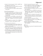
Inject an RF signal from the signal generator at +1.0
dBµ on 145.000 MHz.
Summary of Contents for FT-100 Micro Mobile
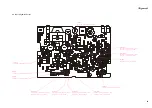
Page 12: ...12 Alignment Note ...
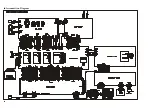
Page 17: ...17 Block Diagram ...
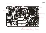
Page 18: ...18 Interconnection Diagram ...
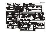
Page 19: ...19 Circuit Diagram MAIN Unit Lot 1 4 ...
Page 20: ...20 MAIN Unit Lot 1 4 Note ...
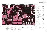
Page 23: ...23 MAIN Unit Lot 5 Circuit Diagram ...
Page 24: ...24 MAIN Unit Lot 5 Note ...
Page 51: ...51 Circuit Diagram Parts Layout Side A Side B DAN235U M D1801 1802 1803 1804 BPF Unit ...
Page 52: ...52 BPF Unit Lot 9 Circuit Diagram Parts Layout Side A Side B DAN235U M D1801 1802 1803 1804 ...
Page 54: ...54 BPF Unit Note ...
Page 55: ...55 Circuit Diagram Parts Layout Side A Side B 2SC4047 ZY Q1901 1902 HPF Unit ...
Page 56: ...56 HPF Unit Lot 6 Circuit Diagram Parts Layout Side A Side B DTC114EU 24 Q1901 1902 1903 ...
Page 58: ...58 HPF Unit Note ...
Page 59: ...59 Circuit Diagram Parts Layout NJM2904V Q1951 1952 Audio Filter Unit Side A Side B ...
Page 60: ...60 Audio Filter Lot 6 Circuit Diagram Parts Layout Side A Side B NJM2904V Q1951 1952 ...
Page 62: ...62 Audio Filter Unit Note ...
Page 63: ...63 Local Unit Circuit Diagram ...
Page 74: ...74 Local Unit Note ...
Page 75: ...75 REF Unit Circuit Diagram Parts Layout Side A Side B 2SC2714Y QY Q2801 2802 ...
Page 77: ...77 PA Unit Circuit Diagram ...
Page 78: ...78 PA Unit Note ...
Page 88: ...88 PA Unit Note ...
Page 89: ...89 Circuit Diagram LPF Unit ...
Page 91: ...91 Circuit Diagram LPF Unit Lot 9 ...
Page 98: ...98 LPF Unit Note ...
Page 99: ...99 Circuit Diagram Display Unit Lot 1 ...
Page 101: ...101 Circuit Diagram Display Unit Lot 34 ...
Page 106: ...106 Display Unit Note ...
Page 107: ...107 Circuit Diagram CNTL Unit Lot 1 3 ...
Page 109: ...109 CNTL Unit Lot 4 Circuit Diagram ...
Page 116: ...116 CNTL Unit Note ...

