


XC4000 Series Field Programmable Gate Arrays
4-34
September 18, 1996 (Version 1.04)
F1
C1
G1
F2 C2 G2
F3
C3
G3
F4 C4 G4
K
X
Y
XQ
YQ
LONG
SINGLE
DOUBLE
LONG
GLOBAL
QUAD
LONG
SINGLE
DOUBLE
LONG
LONG
DOUBLE
DOUBLE
QUAD
GLOBAL
Common to XC4000E and XC4000EX
XC4000EX only
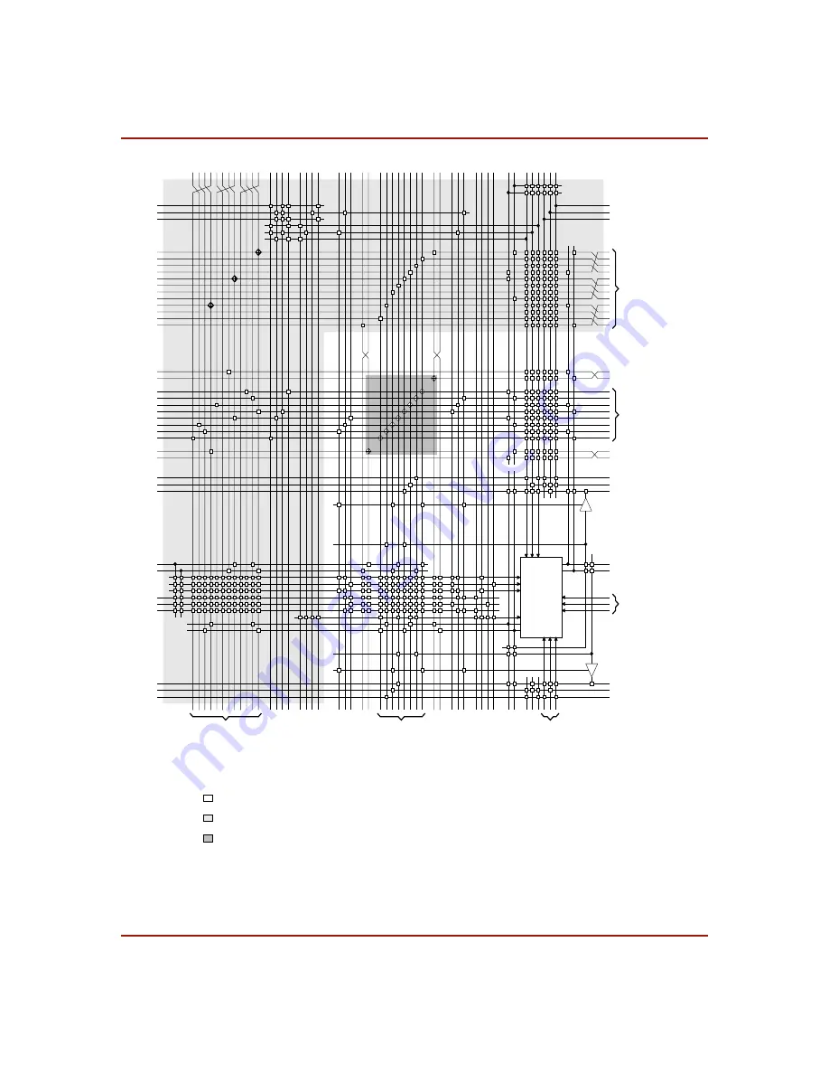
Programmable Switch Matrix
CLB
DIRECT
FEEDBACK
DIRECT
FEEDBACK
Figure 27: Detail of Programmable Interconnect Associated with XC4000-Series CLB


