Ethernet 1000BASE-X PCS/PMA or SGMII v7.0
www.xilinx.com
43
UG145 January 18, 2006
SGMII Example Design / Dynamic Switching Example Design
R
project_dir>
/
<component_name>
/example_design/
sgmii_adapt/
sgmii_adapt.vhd
Verilog
project_dir>
/
<component_name>
/example_design/
sgmii_adapt/
sgmii_adapt.v
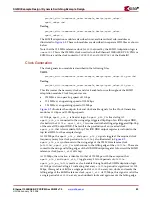
The SGMII adaptation module is described in several hierarchical sub-modules as
illustrated in
Figure 4-8
. These sub-modules are described in separate HDL files as shown
below.
Note that the 125 MHz reference clock (
clk125m
) used by the SGMII Adaptation logic is
userclk2
. This is the 125 MHz clock used to clock the Ethernet 1000BASE-X PCS/PMA or
SGMII core and the clock routed to
TXUSRCLK2
and
RXUSRCLK2
of the RocketIO.
Clock Generation
The clock generation module is described in the following files:
VHDL
project_dir>
/
<component_name>
/example_design/
sgmii_adapt/clk_gen.vhd
Verilog
project_dir>
/
<component_name>
/example_design/
sgmii_adapt/clk_gen.v
This file creates the necessary clocks and clock enables for use throughout the SGMII
adaptation module. Clock frequencies are:
•
125 MHz at an operating speed of 1 Gbps
•
12.5 MHz at an operating speed of 100 Mbps
•
1.25 MHz at an operating speed of 10 Mbps
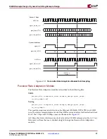
Figure 4-9
illustrates the output clock and clock enable signals for the Clock Generation
module at 1 Gbps and 100 Mbps speeds.
At 1 Gbps,
sgmii_clk_r
is fixed at logic 0;
sgmii_clk_f
is fixed at logic 1.
sgmii_clk_r
is connected to the rising edge triggered flip-flop of an IOB output DDR,
clocked with
clk125m. sgmii_clk_f
is connected to the falling edge triggered flip-flop
of the same IOB output DDR. The result is the production of an inverted clock,
sgmii_clk
, that is forwarded off-chip. This IOB DDR output register is included in the
top level HDL for the example design.
At 100 Mbps, the
sgmii_clk_r
and
sgmii_clk_f
signals toggle at the required clock
frequency (every five clock periods of
clk125m
), also illustrated in
Figure 4-9
.
sgmii_clk_r
is synchronous to the rising edge of the 125 MHz reference clock
(
clk125m)
;
sgmii_clk_f
is synchronous to the falling edge of the
clk125m.
These are
routed to the rising and falling edges of the IOB DDR output register to forward the SGMII
reference clock (
sgmii_clk
) off chip.
At 10 Mbps, the situation is identical to that of 100 Mbps, with the exception that
sgmii_clk_r
and
sgmii_clk_f
toggle every 50 clock periods of
clk125m
.
sgmii_clk_en_fall
is used as a clock enable throughout the SGMII adaptation logic.
At 1 Gbps it is fixed at logic 1 indicating that every
clk125m
period is significant. At 100
Mbps, this signal is valid for a single period of
clk125m
every ten clocks and marks the
falling edge of the SGMII reference clock,
sgmii_clk
. At 10 Mbps, this signal is valid for
a single period of
clk125m
every one hundred clocks and again marks the falling edge


