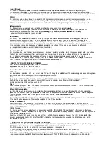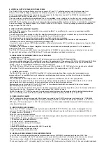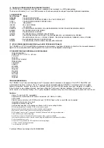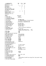
modulation is rather long to avoid visible variations of the signal amplitude, lo improve me speed 01 me AUU system a circuit has
been included which detects whether the AGC detector is activated every frame period. When during 3 frame periods no action is
detected the speed of the system is increased. For signals without peak white information the system switches automatically to a
gated black level AGC. Because a black level clamp pulse is required (or this way of operation the circuit will only switch to black level
AGC in the internal mode.
The circuits contain a video identification circuit which is independent of the synchronisation circuit. Therefore search tuning is
possible when the display section of the receiver is used as a monitor. The ident output is supplied to the tuning system via
the PC-bus. The video ident circuit can be made less sensitive by means of the STM bit. This mode can be used during search tuning
to avoid that the tuning system will stop at very weak input signals.
2.2. Video Switches
The circuits have two CVBS inputs (internal and external CVBS) and Y/C input. When the Y/C input is not required the Y input can be
used as third CVBS input. The selection of the various sources is made via the PC-bus. The circuit has one CVBS output.
2.3. Sound Circuit
The sound band pass and trap filters have to be connected externally. The filtered intercarrier signal is fed to a limiter circuit
and is demodulated by means of a PLL demodulator. This PLL circuit tunes itself automatically to the incoming carrier signal
so that no adjustment is required.
The volume is controlled via the PC-bus. The deemphasis capacitor has to be connected externally. The non-controlled audio
signal can be obtained from this pin. The FM demodulator can be muted via the PC-bus. This function can be used to switch-off
the sound during a channel change so that high output peaks are prevented. The TDA8840/8842 contain an automatic volume
levelling (AVL) circuit which automatically stabilises the audio output signal to a certain level which can be set by the viewer by means
of the volume control. This function prevents big audio output fluctuations due to variations of the modulation depth of the transmitter.
The AVL function can be activated via the PC-bus.
2.4. Synchronisation circuit
The sync seperator is preceded by a controlled amplifier which adjusts the sync pulse amplitude to a fixed level. These pulses are fed
to the slicing stage which is operating at 50% of the amplitude. The separated sync pulses are fed to the first phase detector and to the
coincidence detector. This coincidence detector is used to detect whether the line oscillator is synchronised and can also be used for
transmitter identification. The first PLL has a very high statical steepness so that the phase of the picture is independent of the line
frequency.
The horizontal output signal is generated by means of an oscillator which is running at twice the line frequency. Its frequency is divided
by 2 to lock the first control loop to the incoming signal. The time-constant of the loop can be forced by the PC-bus (fast or slow).
If required the 1C can select the time-constant depending on the noise content of the incoming video signal.
To protect the horizontal output transistor, the horizontal drive is immediately switched off when a power-on-reset is detected.
The drive signal is switched-on again when the normal switch-on procedure is followed.
Via the PC-bus, adjustments can be made of the horizontal and vertical geometry. The vertical sawtooth generator drives the
vertical output drive circuit which has a differential output current. For the EW drive a single ended current output is available.
When the horizontal scan is reduced to display 4 : 3 pictures on a 1 6 : 9 picture tube an accurate video blanking can be switched on
to obtain well defined edges on the screen.
Overvoltage conditions can be detected via the EHT tracking pin.When an overvoKage condition is detected the horizontal output
drive signal will be switched-off via the slow stop procedure but it is also possible that the drive is not switched-off and that just a
protection indication is given in the PC-bus output byte. The choice is made via the input bit PRO.
2.5. Chroma and Luminance processing
The circuits contain a chroma bandpass and trap circuit. The filters are realised by means of gyrator circuits and they are
automatically calibrated by comparing the tuning frequency with the X-tal frequency of the decoder.
The luminance delay line and the delay for the peaking circuit are also realised by means of gyrator circuits.
The centre frequency of the chroma bandpass filter is switchable via the PC-bus so that the performance can be optimised for
"front-end" signals and external CVBS signals.
During SECAM reception the centre frequency of the chroma trap is reduced to get a better suppression of the SECAM
carrier frequencies.
2.6. Colour Decoder
The decoder contains an alignment-free X-tal oscillator, a killer circuit and two colour difference demodulators. The 90° phase shift for
the reference signal is made internally.
The 1C contains an automatic colour limiting (ACL) circuit which prevents that oversaturation occurs when signals with a high
chroma-to-burst ratio are received. The ACL circuit is designed such that it only reduces the chroma signal and not the burst signal.
This has the advantage that the colour sensitivity is not affected by this function.
The base-band delay line is integrated in the PAL/SECAM 1C' s.
The demodulated colour difference signals are internally supplied to the delay line. The matrixed signals are externally available.
The colour difference matrix switches automatically between
PAL/SECAM and NTSC, however, it is also possible to fix the matrix in the PAL standard.
Which colour standard the 1C can decode depends on the external X-tals. The X-tal to be connected to pin 34 must have a frequency
of 3.5 MHz (NTSC-M, PAL-M or PAL-N) and pin 35 can handle X-tals with a frequency of 4.4 and 3.5 MHz. To prevent calibration
problems of the horizontal oscillator the external switching between the 2 X-tals should be carried out when the oscillator is forced to
pin 35. For a reliable calibration of the horizontal oscillator it is very important that the X-tal indication bits (XA and XB) are not
corrupted. For this reason the X-tal bits can be read in the output bytes so that the software can check the W-bus transmission.
2.7. RGB output circuit and black-current stabilisation
The colour-difference signals are matrixed with the luminance signal to obtain the RGB-signals. The TDA 884X device has one linear
RGB input. This RGB signal can be controlled on contrast and brightness.
The output signal has an amplitude of about 2 volts black-to-white at nominal input signals and nominal settings of the controls.
To increase the flexibility of the 1C it is possible to insert OSD and/or teletext signals directly at the RGB outputs.
This insertion mode is controlled via the insertion input (pin 26 in the S-DIP 56- and pin 38 in the QFP-64 level). This blanking action
at the RGB outputs has some delay which must be compansated externally.
To obtain an accurate biasing of the picture tube a "Continuous Cathode Calibration" circuit has been developed.
This function is realised by means of a 2-point black level stabilisation circuit.
When the TV receiver is switched-on, the RGB output signals are blanked and the black current loop will try to set the right picture
tube bias levels. Via the AST bit a choice can be made between automatic start-up or a start-up via the m-processor.
Summary of Contents for 11AK19
Page 1: ...SERVICE MANUAL CHASSIS 11 AK19 FIRMEN EUROLINE PALLADIUM S E G TECHLINE VESTEL...
Page 27: ...GENERAL BLOCK DIAGRAM OF CHASSIS AK19 26...
Page 30: ......
Page 31: ......
Page 32: ......
Page 33: ......
Page 34: ......
Page 35: ......
Page 36: ......
Page 37: ......
Page 38: ......
Page 39: ......


