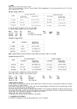
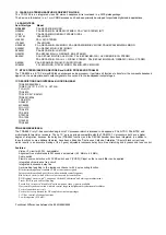
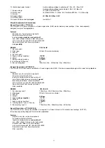
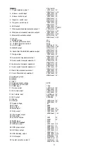


32. External audio input left channel
33. SCART 1 input right channel
34. SCART 1 input left channel
35. Ground guards
36. SCART 2 input right channel
37. SCART 2 input left channel
38. Analogue supply voltage 2
39. Positive reference voltage
40. Reference voltage ground
4 1 . Filter capacitor pin 1
42. Filter capacitor pin 2
43. Analogue supply ground 2
44. Filter capacitor pin 2
45. Filter capacitor pin 1
46. Reference voltage 2
47. Scan 1 output right channel
48. Scart 1 output left channel
49. Digital supply ground 2
50. Analogue supply ground 4
5 1 . Scart 2 output right channel
52. Scart 2 output left channel
53. Reference voltage 3
54. Post-filter capacitor pin right channel
55. Post-filter capacitor pin left channel
56. Analogue supply ground 3
57. Headphone output right channel
58. Headphone output left channel
59. Analogue supply voltage 3
60. Loudspeaker (main) output right channel
61. Loudspeaker (main) output left channel
62. Line output left channel
63. Line output right channel
64. Digital supply voltage 2
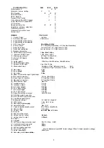
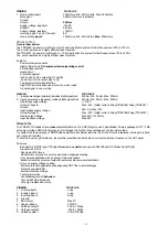
350mVrms
350mVrms
350mVrms
350mVrms
350mVrms
5V, Min : 4.75V, Max : 5.5V
0V
0V
Vdda2/Vssa2 : 50%
500mVrms
500mVrms
0V
0V
500mVrms
500mVrms
Vdda3/Vssa3:50%
0V
Vo(clip): Min : 1400mVrms
Vo(clip) : Min : 1400mVrms
5.0V, Min : 4.75V, Max : 5.5V
Vo(clip) : Min : 1400mVrms
Vo(clip): Min : 1400mVrms
500mVrms
500mVrms
5.0V, Min : 4.75V, Max: 5.5V
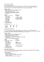
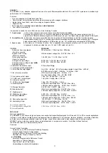
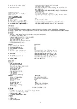
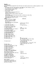
TDA9818:
General description:
The TDA9818 is an integrated circuit for multistandard vision IF signal processing, sound AM and FM demodulation.
Features:
• 5 V supply voltage
• Applicable for IF frequencies of 38.9 MHz, 45.75 MHz and 58.75 MHz
• Gain controlled wide band VIF-amplifier (AC-coupled)
• True synchronous demodulation with active carrier regeneration (very linear demodulation, good intermodulation figures, reduced
harmonics, excellent pulse response)
• Robustness for ove modulation better than 105% due to gated phase detector at L/L accent standard and PLL-bandwidth control
at negative modulated standards
• VCO frequency switchable between L and L accent (alignment external) picture carrier frequency
• VI F AGC detector for gain control, operating as peak sync detector for B/G, peak white detector for L; signal controlled reaction
time for L
• Tuner AGC with adjustable takeover point (TOP)
• AFC detector without extra reference circuit
• AC-coupled limiter amplifier for sound intercanrier signal
• Alignment-free FM-PLL demodulator with high linearity
• SIF input for single reference QSS mode (PLL controlled); SIF AGC detector for gain controlled SIP amplifier; single reference
QSS mixer able to operate in high performance single reference QSS mode and in intercarrier mode
• AM demodulator without extra reference circuit
• Stabilizer circuit for ripple rejection and to achieve constant output signals
• ESD protection for all pins
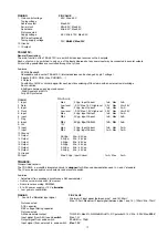
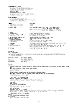
PIN VALUE
PINNING
1 . VIF differential input signal voltage 1
2. VIP differential input signal voltage 2
3. Standard switch
4. VIF AGC capacitor
Input signal voltage sensitivity
60m Vims, Max:100mVrms
Input signal voltage sensitivity
60mVnns, Max:100mVrms
Min : 2.8V, Max : Vp
Charging current: 1 mA, Min : 0.75mA, Max : 1.25mA
Discharging current: B/G standard : 20mA, Min : 15mA, Max:25mA
Normal mode L : 300nA, Min : 225nA, Max : 375nA
Fast mode L : 40mA, Min : 30mA, Max : 50mA
Charging current: FM mode : 12mA, Min : 8mA, Max : 16mA
5. SIP AQC capacitor
AM mode : 1.2mA, Min : 0.8mA, Max : 1.6mA
Discharging current: FM mode : 12mA, Min : 8mA, Max: 16mA
Normal mode AM : 1.4mA, Min : 1mA, Max : 1.8mA
Fast mode AM : 85mA, Min : 60mA, Max: 110mA
Min:0V, Max:Vp
PLL loop filter
L/L accent switch and adjust
Audio output
Min:0V, Max:Vp
Rx : 470ohm : 250mVrms, Min : 200mVrms, Max : 300mVrms
Rx: Oohm : 500mVrms, Min : 400mVrms, Max : 600mVrms
Min:0V, Max:Vp
9. De-emphasis input
10. De-emphasis output
1 1 . Decoupling capacitor
12. Single reference QSS/intei-can-ier output voltage
Min:0V, Max:Vp
Min:0V, Max:Vp
140m Vims, Min : 100mVrms Max : 180mVnns
17
Summary of Contents for 11AK19
Page 1: ...SERVICE MANUAL CHASSIS 11 AK19 FIRMEN EUROLINE PALLADIUM S E G TECHLINE VESTEL...
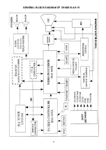
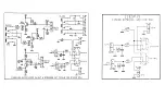
Page 27: ...GENERAL BLOCK DIAGRAM OF CHASSIS AK19 26...
Page 30: ......
Page 31: ......
Page 32: ......
Page 33: ......
Page 34: ......
Page 35: ......
Page 36: ......
Page 37: ......
Page 38: ......
Page 39: ......