background image

1-10

VX-4000 UHF Service Manual

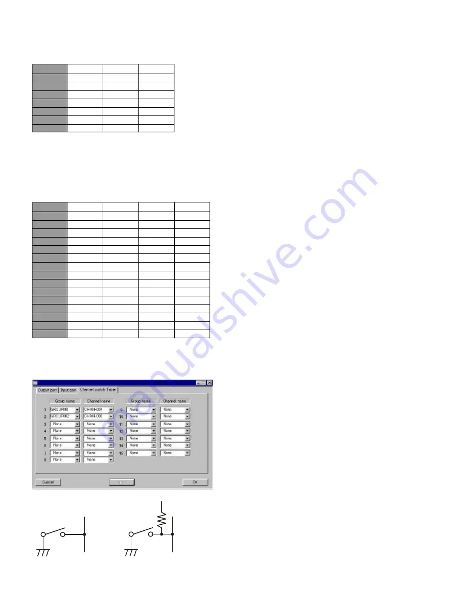
Similarly, if you assign “CH SW0,” “CH SW1,”

and “CH SW2” to the Universal Input Port, you

can recall Channels 1~7 as shown below:

The Memory Channel is determined via the CE35

Programmer. (View 

à

 Common View 

à

 DSUB-

25pin connector 

à

 Channel switch Table).

Pin 7: E 

[GND]

Ground for all logic levels and power supply re-

turn.

Pin 8: AO2 

[Universal Output Port]

Open collector output. Output voltage 0 ~ 5 V,

Max. sink current 30 mA.

The possible programming features (use CE35)

are illustrated below.

A KEY

/

B KEY

/

C KEY

/

D KEY

/

E KEY

/

HA

/

Invert

Refer to the “Pins 20, 21, & 22” section for details.

Pin 9: TXD2 

[Digital Output for Alignment software]

Connect to the RS232C cable (requires FIF-8 and

CT-88)

Pin 10: RXD2 

[Digital Input for Alignment software]

Connect to the RS232C cable (requires FIF-8 and

CT-88)

Pin 11: TXS 

[EXT PTT]

Shorting this port to ground causes the trans-

ceiver to be placed in the Transmit mode, while

opening the connection to this port returns the

transceiver to the Receive mode.

Pin 12: MCM 

[MIC Mute]

MIC mute on: Level High (5V)

MIC mute off: Open

LOGIC level (+5V / 0V) output.

When the PTT/EXT PTT switch is pressed, this

pin switches to “open.”

Pin 13: MD/DI 

[Digital Input for DATA Communications]

m

TX Hi-speed Data Input Type (jumper JP2006).

Input level 800 mV/600 Ohms, Max.input 1.2V

m

Tx Low-speed Data input Type (Jumper

JP2007). Input level 40 mV/600-Ohms

If the Jumper setting is “Low-speed Data” (JP2007

jumpered), this port is usable in the AUDIO

(300~3000 Hz) range.

If the jumper setting is “HI-speed Data” (JP2006

jumpered), this port is usable for 9600 bps DATA

communications, because the filter and limiter are

not engaged in the Audio line.

Pin 14: SB 

[13.8 V/5 V DC Output]

m

Switched 13.8V output for supplying power

to an accessory (jumper JP2009).

m

Switched and regulated DC 5.0V output for

supplying power to an accessory (jumper

JP2008).

Maximum output current is 200 mA

If you need to recall all memory channels (15 CH)

from the External Controller via the Uni-versal

Input Port, you should assign the “All Channel

Recall” Command (CH SW 0 ~ CH SW 3) to the

Universal Input Port.

In this case:

Channel

CH SW0

CH SW1

CH SW2

1

1

0

0

2

0

1

0

3

1

1

0

4

0

0

1

5

1

0

1

6

0

1

1

7

1

1

1

Channel

CH SW0

CH SW1

CH SW2

CH SW3

1

1

0

0

0

2

0

1

0

0

3

1

1

0

0

4

0

0

1

0

5

1

0

1

0

6

0

1

1

0

7

1

1

1

0

8

0

0

0

1

9

1

0

0

1

10

0

1

0

1

11

1

1

0

1

12

0

0

1

1

13

1

0

1

1

14

0

1

1

1

15

1

1

1

1

Sample Circuit

PINS 2, 3, 4, 6

DSUB 25-Pin

PIN 5 (Pull Up)

47k

W

5V

DSUB 25-Pin

Summary of Contents for VX-4000U

Page 1: ...nt Your cooperation in pointing out any inconsistencies in the technical information would be appreciated 2002 VERTEX STANDARD CO LTD Printed in Japan Service Manual VX 4000U UHF FM Transceiver Operating Manual Reprint 1 1 Cloning 2 1 Specifications 2 2 Exploded View Miscellaneous Parts 3 1 Block Diagram 3 2 Interconnection Diagram 3 4 Circuit Description 4 1 Alignment 5 1 Contents Board Unit Sche...

Page 2: ...Button Pressing these buttons changes the current group and displayed group number or name Hold ing this button for more than 1 2 second causes the function to repeat SQC Indicator This lamp glows orange when incorrect position at the setting of CE35 Programmable Function Button PF button This button can be set up for special applications such as high low power selection monitor dim mer talk aroun...

Page 3: ...e jack Caution Do not connect this line to ground and be certain that the speaker has adequate capa bility to handle the audio output from the VX 4000  13 8 V DC Cable Pigtail w Connector The supplied DC power cable must be connected to this 2 pin connector Use only the supplied fused cable extended if necessary for power con nection à DSUB 25 Pin Accessory Connector External TX audio line input ...

Page 4: ...or the desired audio level Press and hold the MON button more than 1 2 seconds to quiet the noise and resume normal quiet monitoring Transmitting To transmit wait until the BUSY indicator is off the channel is not in use and press the PTT Push To Talk switch on the side of the micro phone the TX indicator will appear or the TX indicator will glow red While holding in the PTT switch speak across th...

Page 5: ... on next page For further details contact your VERTEX STAN DARD dealer For future reference check the box next to each function that has been assigned to the PF button on your particular radio and keep it handy 1 5 sec 1 5 sec 1 5 sec 1 5 sec 1 5 sec 1 5 sec 1 5 sec 1 5 sec 1 5 sec 1 5 sec 1 5 sec 1 5 sec 1 5 sec 1 5 sec Functions Programmable Function Button PF button None SCAN SCN Dual Watch Cal...

Page 6: ...unication range During ARTS operation your radio automatically transmits for about 1 second every 25 or 55 sec onds the interval is programmed by Dealer in an attempt to Shake hands with the other station If you move out of range for more than one min utes your radio senses that no signal has been received a ringing beeper will sound If you sub sequently move back into range as soon as the other s...

Page 7: ...ars on the display The in tercom can be used even while scanning and re ceiving a call Low Power Press the assigned PF button of the Low Power to set the radio s transmitter to the Low Power mode Press this key again to return to High Power operation when in difficult terrain ADVANCED OPERATION GRP UP DWN Press the assigned PF button of the GRP UP or GRP DWN to select a different group of chan nel...

Page 8: ...one sounds and SQL appears on the display with the current squelch level 2 Rotate the CHANNEL selector knob to select the desired level 3 Press the this key A tone sounds and the dis play returns to the normal channel Encryption Option When the Voice Scrambler feature is enabled pressing the assigned PF button of the Encryp tion toggles the Scrambler on and off ADVANCED OPERATION ...

Page 9: ...Deck w MMB 75 for Dual Band Installations RMK 4000SH Remote Kit for Single Transceiver RMK 4000DH Remote Kit for Dual Head Installations RMK 4000DB Remote Kit for Dual Band Installations RMK 4000DBH Remote Kit for Dual Band plus Dual Head Installations F2D 8 2 Tone Decode Unit Requires FIF 7 F5D 14 5 Tone ENC DEC Unit Requires FIF 7 VTP 50 VX Trunk Unit Requires FIF 7 FVP 25 Encryption DTMF pager ...

Page 10: ...To select the Input port page View à Com mon View à DSUB 25pin connector à Input port LOGIC level 5V 0V input Low active High Impedance input None MON This feature is the same as pressing and holding in the Monitor key DIM LCD illumination dimmer on Hook Activates the Hook1 feature SCAN Activates the scanner G SCAN Activates the Group scanner RPT INH Disables the repeater feature during Multi Deck...

Page 11: ...sed this pin switches to open Pin 13 MD DI Digital Input for DATA Communications m TX Hi speed Data Input Type jumper JP2006 Input level 800 mV 600 Ohms Max input 1 2V m Tx Low speed Data input Type Jumper JP2007 Input level 40 mV 600 Ohms If the Jumper setting is Low speed Data JP2007 jumpered this port is usable in the AUDIO 300 3000 Hz range If the jumper setting is HI speed Data JP2006 jumpere...

Page 12: ...d in the Audio line Pin 18 E GND Ground for all logic levels and power supply re turn Pin 19 NC No Connection Pins 20 21 22 AO1 AO3 AO4 Universal Output Port LOGIC level 5V 0V output The logic output appears at these pins when the front panel s PF key is turned on The possible programming features use CE35 are illustrated below If the HA feature is assigned to these ports a cur rent amplifier must...

Page 13: ...n Data will now be transferred to the Destina tion transceiver from the source transceiver 6 If there is a problem during the cloning process sound an error beep from source the transceiver Check your cable connections and battery volt age and try again 7 If cloning is a successful turn the Destination transceiver off Now turn the source transceiv er off 8 Disconnect the CT 72 Replace the plastic ...

Page 14: ...standard TIA EIA 603 Circuit Type Double conversion Super heterodyne Sensitivity EIA 12 dB SINAD 0 25 µV Adjacent Channel Selectivity 80 dB 70 dB Intermodulation 76 dB Spurious and Image Rejection 90 dB Audio Response 3 8 dB from the 6 dB oct re emphasis curve Audio Output 5 W 4 Ohms 10 THD 10 W 4 Ohms w 10 THD Option TRANSMITTER Measurements made per EIA standard TIA EIA 603 Power Output 40 25 W ...

Page 15: ...90 HOLDER RA0251500 CHASSIS Q6000114 TERMINAL STRIP S6000396 RUBBER GROMMET TM 96 17 S6000395 COVER P 25P 23 Á É Ã Ã Ã Ã Ã Ã Ã Ã Ã Ã Á Á Á À À À Â Â Â Â Â Â Â Â Ä Å Á Á Æ È RA02543A0 KNOB Ã Ã P1090984 CONNECTOR MIC CONN Unit Non designated parts are available only as part of a designated assembly Accessories Description VXSTD P N Qty BLADE FUSE ATC 15A Q0000075 2 DC CABLE 02P 15AX2 T9021015 1 KNOB...

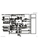
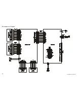
Page 16: ...VX 4000 UHF Service Manual 3 2 Block Diagram ...

Page 17: ...VX 4000 UHF Service Manual 3 3 Block Diagram ...

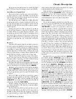
Page 18: ...VX 4000 UHF Service Manual 3 4 Interconnection Diagram ...

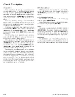
Page 19: ...50 kHz by the 2nd mixer and stripped of unwant ed components by ceramic filter CF1001 or CF1002 After passing through a limiter amplifier the signal is demodulated by the FM detector Demodulated receive audio from the IF IC is amplified by Q2014 CXA1846N After volume ad justment by the AF power amplifier Q2029 TDA7240AV the audio signal is passed to the op tional headphone jack or 4 ohm loudspeake...

Page 20: ...4V Q1001 2SC4154E Q1002 2SB1143S to transmitter RF amplifier and thus the power output Generation of spurious products by the transmit ter is minimized by the fundamental carrier frequen cy being equal to the final transmitting frequency modulated directly in the transmit VCO Addition al harmonic suppression is provided by a low pass filter consisting of L1001 L1003 L1004 and C1004 C1008 C1009 C10...

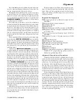
Page 21: ...ng test equipment and thorough familiarity with its correct use is neces sary for complete realignment Correction of prob lems caused by misalignment resulting from use of improper test equipment is not covered under the warranty policy While most steps do not require all of the equip ment listed the interactions of some adjustments may require that more complex adjustments be per formed afterward...

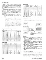
Page 22: ...SS DCS Narrow wide simplex Encode Encode CH1 400 01 MHz None None Wide CH2 415 01 MHz None None Wide CH3 429 99 MHz None None Wide CH4 400 01 MHz None None Narrow CH5 415 01 MHz None None Narrow CH6 429 99 MHz None None Narrow CH7 415 01 MHz 151 4 Hz None Wide CH8 415 01 MHz None 023 Wide CH9 415 01 MHz 151 4 Hz None Narrow CH10 415 01 MHz None 023 Narrow UHF TYPE D Channel Frequency CTCSS DCS Nar...

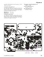
Page 23: ...the onboard help of the Align ment Software Manual for details HIGH Power 50 1 W LOW Power 25 0 5 W Transmitter Deviation The following modulation parameters can be ad justed from the computer by utilizing the Alignment Software Refer to the onboard help of the Align ment Software Manual for details TP1007 L1016 L1017 TC1001 Microphone Audio Modulation Level 4 3 kHz 0 1 kHz CTCSS Modulation Level ...

Page 24: ... 0 45V 0 00V 4 84V 0 0V 8 44V 2 05V 1 74V 2 23V 4 5V 1 62V 1 36V 2 73V 2 92V 4 8V 4 9V 0V 4 84V 4 87V XX TX 465 00 MHz MIC Input Level 1 kHz 3 0mV STD Dev High Power XX RX 465 10 MHz RF Input Level 40dbµ emf MOD 1 0 kHz Dev 3 0 kHz EXT SP OUT 10 Distn 14 0W 6 81V 0 0V 1 35V 0 0V 2 19V 0 0V 2 62V 0 0V 0 0V 5 67V 1 02V 0 0V 8 74V 0 0V 0 71V 0 0V 0 55V 3 88V 4 72V 4 72V 0 69V 0 69V 2 12V 0V 7 41V 0V ...

Page 25: ...V 4 86V 4 76V 0 0V 2 12V 2 12V 2 4V 2 41V 2 38V 2 38V 2 4V 2 4V 0 0V 0 0V 4 03V 4 03V 4 03V 4 03V 4 04V 4 04V 4 54V 4 5V 4 5V 4 5V 4 5V 8 97V 8 97V 3 85V 3 85V 3 84V 3 84V 3 85V 3 85V 3 84V 3 85V 8 65V 8 65V 8 96V 8 97V 2 14V 2 14V 2 22V 2 22V 0 0V 4 06V 0 14V 2 03V 0 0V 2 03V 0 0V 3 6V 0 01V 0 81V 1 28V 1 1V 8 64V 8 65V 0 01V 0 78V 0 0V 0 77V 1 31V 1 1V 1 86V 1 19V 1 1V 1 1V 1 76V 1 18V 1 1V 1 1V...

Page 26: ... 2SC5107 O MFO Q1018 2SC4227 R34 Q1012 2SC4226 R24 Q1014 2SC4116GR LG Q1033 RT1N241M N2 Q1004 1016 1032 2006 2011 2116 2119 2124 IMH6 H6 Q1009 1017 3SK228 XR Q1025 2SK508 K52 Q1015 TA31136FN Q1026 BU4066BF Q2007 DTC323TK H02 Q2012 CXA1846N Q2014 HN58X2432TI Q2028 IMD3 D3 Q2112 TC4W53FU Q2117 MB90F583B Q2019 SA7025DK Q1024 TDA7240AV Q2029 M68769H 01 Q1013 ...

Page 27: ...2 IMX1 X1 Q2009 S 80735SN DZ Q2027 IMD3 D3 Q2115 2SC4154E LE Q1008 2SC5107 O MFO Q1019 1021 1031 2SC4116GR LG Q1027 2SC4215Y QY Q1029 2SB1132R BA Q1006 2SC2954 QK Q1020 2SC5415E EA Q1022 2SA1602A MF Q2025 MC2850 A7 D1033 2002 2006 2010 HSM88AS C1 D1011 1014 1SS321 F9 D1024 MC2848 A6 D1026 1028 MC2846 D2001 2007 2SB1143S Q1002 2SB1201STP Q1003 MX165CDW Q2013 2SJ327Z Q2020 M5223AGP Q1007 NJM2902V Q2...

Page 28: ... 0 45V 0 00V 4 84V 0 0V 8 44V 2 05V 1 74V 2 23V 4 5V 1 62V 1 36V 2 73V 2 92V 4 8V 4 9V 0V 4 84V 4 87V XX TX 465 00 MHz MIC Input Level 1 kHz 3 0mV STD Dev High Power XX RX 465 10 MHz RF Input Level 40dbµ emf MOD 1 0 kHz Dev 3 0 kHz EXT SP OUT 10 Distn 14 0W 6 81V 0 0V 1 35V 0 0V 2 19V 0 0V 2 62V 0 0V 0 0V 5 67V 1 02V 0 0V 8 74V 0 0V 0 71V 0 0V 0 55V 3 88V 4 72V 4 72V 0 69V 0 69V 2 12V 0V 7 41V 0V ...

Page 29: ...V 4 86V 4 76V 0 0V 2 12V 2 12V 2 4V 2 41V 2 38V 2 38V 2 4V 2 4V 0 0V 0 0V 4 03V 4 03V 4 03V 4 03V 4 04V 4 04V 4 54V 4 5V 4 5V 4 5V 4 5V 8 97V 8 97V 3 85V 3 85V 3 84V 3 84V 3 85V 3 85V 3 84V 3 85V 8 65V 8 65V 8 96V 8 97V 2 14V 2 14V 2 22V 2 22V 0 0V 4 06V 0 14V 2 03V 0 0V 2 03V 0 0V 3 6V 0 01V 0 81V 1 28V 1 1V 8 64V 8 65V 0 01V 0 78V 0 0V 0 77V 1 31V 1 1V 1 86V 1 19V 1 1V 1 1V 1 76V 1 18V 1 1V 1 1V...

Page 30: ...001uF 50V B GRM39B102K50PT K22174821 1 A B2 C 1014 FILM CAP 5pF 500V UC232H0050D T K33279010 1 2 A F2 C 1014 FILM CAP 5pF 500V UC232H0050D T K33279010 VERSION A 3 A F2 C 1014 FILM CAP 5pF 500V UC232H0050D T K33279010 VERSION D 3 A F2 C 1014 FILM CAP 4pF 500V UC232H0040D T K33279044 VERSION F 4 A F2 C 1015 CHIP CAP 0 001uF 50V B GRM39B102K50PT K22174821 1 A B2 C 1016 CHIP CAP 5pF 50V CH GRM39CH050C...

Page 31: ... 1 B b2 C 1059 CHIP CAP 470pF 50V CH GRM39CH471J50PT K22174249 1 B b2 C 1061 CHIP CAP 0 001uF 50V B GRM42 6B102M50PT K22171801 1 B c2 C 1062 CHIP TA CAP 4 7uF 25V TEMSVB21E475M 8R K78140019 1 B e2 C 1063 CHIP CAP 220pF 50V CH GRM39CH221J50PT K22174243 1 A E5 C 1064 CHIP CAP 6pF 50V CH GRM39CH060D50PT K22174207 1 2 A E5 C 1064 CHIP CAP 7pF 50V CH GRM39CH070D50PT K22174208 VERSION A 3 A E5 C 1064 CH...

Page 32: ...uF 25V B GRM39B103K25PT K22144803 1 A E5 C 1103 CHIP CAP 0 001uF 50V B GRM39B102K50PT K22174821 1 A F3 C 1104 CHIP CAP 220pF 50V CH GRM39CH221J50PT K22174243 1 A F3 C 1106 CHIP CAP 220pF 50V CH GRM39CH221J50PT K22174243 1 2 A F3 C 1106 CHIP CAP 220pF 50V CH GRM39CH221J50PT K22174243 VERSION A 3 A F3 C 1106 CHIP CAP 220pF 50V CH GRM39CH221J50PT K22174243 VERSION D 3 A F3 C 1106 CHIP CAP 10pF 50V CH...

Page 33: ...A E4 C 1149 CHIP CAP 6pF 50V CH GRM39CH060D50PT K22174207 VERSION A 3 A E4 C 1149 CHIP CAP 3pF 50V CJ GRM39CJ030C50PT K22174204 VERSION D 3 A E4 C 1149 CHIP CAP 3pF 50V CJ GRM39CJ030C50PT K22174204 VERSION F 4 A E4 C 1150 CHIP CAP 220pF 50V CH GRM39CH221J50PT K22174243 1 B b5 C 1151 CHIP CAP 4pF 50V CH GRM39CH040C50PT K22174205 1 A E3 C 1152 CHIP CAP 10pF 50V CH GRM39CH100D50PT K22174211 1 A E3 C ...

Page 34: ...IP CAP 0 001uF 50V B GRM39B102K50PT K22174821 1 B b4 C 1193 CHIP CAP 3pF 50V CJ GRM39CJ030C50PT K22174204 1 2 A E5 C 1193 CHIP CAP 3pF 50V CJ GRM39CJ030C50PT K22174204 VERSION A 3 A E5 C 1193 CHIP CAP 3pF 50V CJ GRM39CJ030C50PT K22174204 VERSION D 3 A E5 C 1193 CHIP CAP 2pF 50V CK GRM39CK020C50PT K22174203 VERSION F 4 A E5 C 1195 CHIP CAP 0 001uF 50V B GRM39B102K50PT K22174821 1 A G4 C 1196 CHIP C...

Page 35: ...H GRM39CH471J50PT K22174249 4 A F2 C 1271 CHIP CAP 0 5pF 50V CK GRM39CK0R5C50PT K22174201 VERSION A 3 C 2001 CHIP TA CAP 10uF 10V TEMSVA1A106M 8R K78100028 1 A A1 C 2002 CHIP TA CAP 10uF 10V TEMSVA1A106M 8R K78100028 1 A A1 C 2003 CHIP CAP 100pF 50V CH GRM39CH101J50PT K22174235 1 B g4 C 2004 CHIP CAP 100pF 50V CH GRM39CH101J50PT K22174235 1 A B1 C 2005 CHIP CAP 100pF 50V CH GRM39CH101J50PT K221742...

Page 36: ...RM39CH221J50PT K22174243 1 A C3 C 2059 CHIP CAP 220pF 50V CH GRM39CH221J50PT K22174243 1 A C3 C 2060 CHIP CAP 0 01uF 25V B GRM39B103K25PT K22144803 1 A B4 C 2061 CHIP CAP 0 01uF 25V B GRM39B103K25PT K22144803 1 A B4 C 2062 CHIP TA CAP 4 7uF 10V TEMSVA1A475M 8R K78100022 1 A C5 C 2062 CHIP TA CAP 4 7uF 16V TEMSVA1C475M 8R K78120031 4 A C5 C 2063 CHIP CAP 0 1uF 16V B GRM39B104K16PT K22124805 1 A C5 ...

Page 37: ...9B103K25PT K22144803 1 B f2 C 2114 CHIP CAP 0 01uF 25V B GRM39B103K25PT K22144803 1 A A5 C 2115 CHIP CAP 0 01uF 25V B GRM39B103K25PT K22144803 1 B d5 C 2116 CHIP CAP 0 001uF 50V B GRM39B102K50PT K22174821 1 B g4 C 2117 CHIP CAP 0 022uF 25V B GRM39B223K25PT K22144807 1 B d5 C 2118 CHIP CAP 0 0012uF 50V B GRM39B122M50PT K22174810 1 B d5 C 2119 AL ELECTRO CAP 470uF 16V RE3 16V471M 470UF K40129066 1 A...

Page 38: ...CH GRM39CH101J50PT K22174235 1 A B1 C 2172 CHIP CAP 0 01uF 25V B GRM39B103K25PT K22144803 1 B f3 C 2173 CHIP CAP 0 01uF 25V B GRM39B103K25PT K22144803 1 B f3 C 2174 CHIP CAP 0 01uF 25V B GRM39B103K25PT K22144803 1 B f3 C 2175 CHIP CAP 0 01uF 25V B GRM39B103K25PT K22144803 1 B f3 C 2176 CHIP CAP 470pF 50V CH GRM39CH471J50PT K22174249 1 A A5 C 2177 CHIP CAP 470pF 50V CH GRM39CH471J50PT K22174249 1 A...

Page 39: ...6 G2070716 1 A A5 F 2001 CHIP FUSE 0 25A KAB 2402 251NA31 Q0000085 1 A A1 J 2001 CONNECTOR JBY 25S 1A3F P1090815 1 B f1 J 2004 CONNECTOR BM03B SRSS TBT P0091301 1 A A2 J 2005 CONNECTOR AXN426C530P P0091296 1 A B4 L 1001 COIL 0 015uH AS1203 15NK L0022543 1 2 A G1 L 1001 COIL 0 015uH AS1203 15NK L0022543 VERSION A 3 A G1 L 1001 COIL 0 015uH AS1203 15NK L0022543 VERSION D 3 A G1 L 1001 COIL 0 01uH AS...

Page 40: ... 1 6 4T L L0022456 1 2 A E3 L 1027 COIL E2 0 35 1 6 5 5T L L0022616 VERSION A 3 A E3 L 1027 COIL E2 0 35 1 6 4T L L0022456 VERSION D 3 A E3 L 1027 COIL E2 0 4 1 5 4T L L0022475 VERSION F 4 A E3 L 1028 M RFC 0 015uH HK1608 15NJ T L1690518 1 B e3 L 1029 M RFC 0 047uH HK1608 47NJ T L1690524 1 2 B d3 L 1029 M RFC 0 047uH HK1608 47NJ T L1690524 VERSION A 3 B d3 L 1029 M RFC 0 047uH HK1608 47NJ T L16905...

Page 41: ...E4 Q 1026 IC TA31136FN EL G1091605 1 A G4 Q 1027 TRANSISTOR 2SC4116GR TE85R G3341167G 1 B b4 Q 1028 TRANSISTOR RT1N241M T11 1 G3070249 1 B a5 Q 1029 TRANSISTOR 2SC4215Y TE85R G3342157Y 1 B a4 Q 1030 IC MM1216ENRE G1092432 1 B e3 Q 1031 TRANSISTOR 2SC5107 O TE85R G3351077O 1 B e3 Q 1032 TRANSISTOR RT1N241M T11 1 G3070249 1 A G4 Q 1033 TRANSISTOR 2SC4116GR TE85R G3341167G 1 A C3 Q 2001 IC NJM2902V T...

Page 42: ...G 1SJ121P 120 J22309011 1 A E3 R 1017 CHIP RES 220k 1 16W 5 RMC1 16 224JATP J24185224 1 B d2 R 1018 CHIP RES 15k 1 16W 5 RMC1 16 153JATP J24185153 1 A D3 R 1019 CHIP RES 10k 1 16W 5 RMC1 16 103JATP J24185103 1 A D3 R 1020 CHIP RES 1 2k 1 16W 5 RMC1 16 122JATP J24185122 1 B d3 R 1021 CHIP RES 2 2k 1 16W 5 RMC1 16 222JATP J24185222 1 B e3 R 1023 CHIP RES 100k 1 16W 5 RMC1 16 104JATP J24185104 1 A F3...

Page 43: ...6W 5 RMC1 16 121JATP J24185121 1 B c4 R 1081 CHIP RES 10k 1 16W 5 RMC1 16 103JATP J24185103 1 A F5 R 1082 CHIP RES 56 1 16W 5 RMC1 16 560JATP J24185560 1 B c4 R 1083 CHIP RES 22 1 16W 5 RMC1 16 220JATP J24185220 1 B b5 R 1084 CHIP RES 100 1 16W 5 RMC1 16 101JATP J24185101 1 B e2 R 1086 CHIP RES 100 1 16W 5 RMC1 16 101JATP J24185101 1 A D3 R 1087 CHIP RES 1k 1 16W 5 RMC1 16 102JATP J24185102 1 B d4...

Page 44: ... 16W 5 RMC1 16 150JATP J24185150 1 B d3 R 1150 CHIP RES 220 1 16W 5 RMC1 16 221JATP J24185221 1 B d3 R 1151 CHIP RES 220 1 16W 5 RMC1 16 221JATP J24185221 1 B d3 R 1152 CHIP RES 1k 1 16W 5 RMC1 16 102JATP J24185102 1 B e2 R 1153 CHIP RES 2 2k 1 16W 5 RMC1 16 222JATP J24185222 1 B d2 R 1154 CHIP RES 68 1 16W 5 RMC1 16 680JATP J24185680 1 A C3 R 1155 CHIP RES 22 1 10W 5 RMC1 10T 220J J24205220 1 B e...

Page 45: ... 10k 1 16W 5 RMC1 16 103JATP J24185103 1 A C5 R 2061 CHIP RES 100k 1 16W 5 RMC1 16 104JATP J24185104 1 B e5 R 2062 CHIP RES 0 1 16W 5 RMC1 16 000JATP J24185000 1 B f3 R 2063 CHIP RES 10k 1 16W 5 RMC1 16 103JATP J24185103 1 B e4 R 2064 CHIP RES 15k 1 16W 5 RMC1 16 153JATP J24185153 1 B e4 R 2065 CHIP RES 1k 1 16W 5 RMC1 16 102JATP J24185102 1 A A3 R 2066 CHIP RES 10k 1 16W 5 RMC1 16 103JATP J241851...

Page 46: ... 5 RMC1 16 122JATP J24185122 1 B e5 R 2121 CHIP RES 15k 1 16W 5 RMC1 16 153JATP J24185153 1 B e4 R 2122 CHIP RES 470k 1 16W 5 RMC1 16 474JATP J24185474 1 B e5 R 2123 CHIP RES 470k 1 16W 5 RMC1 16 474JATP J24185474 1 B d5 R 2124 CHIP RES 330k 1 16W 5 RMC1 16 334JATP J24185334 1 B d5 R 2125 CHIP RES 330k 1 16W 5 RMC1 16 334JATP J24185334 1 B d5 R 2126 CHIP RES 1M 1 16W 5 RMC1 16 105JATP J24185105 1 ...

Page 47: ...6 473JATP J24185473 1 B f2 R 2193 CHIP RES 47k 1 16W 5 RMC1 16 473JATP J24185473 1 B f3 R 2195 CHIP RES 10k 1 16W 5 RMC1 16 103JATP J24185103 1 B f5 R 2196 CHIP RES 1k 1 16W 5 RMC1 16 102JATP J24185102 1 A B3 R 2197 CHIP RES 33k 1 16W 5 RMC1 16 333JATP J24185333 1 B g3 R 2198 CHIP RES 10k 1 16W 5 RMC1 16 103JATP J24185103 1 A A4 R 2200 CHIP RES 10k 1 16W 5 RMC1 16 103JATP J24185103 1 B d5 R 2201 C...

Page 48: ...P J24185471 1 B f1 R 2257 CHIP RES 0 1 16W 5 RMC1 16 000JATP J24185000 1 B f1 R 2258 CHIP RES 0 1 16W 5 RMC1 16 000JATP J24185000 1 B g1 R 2259 CHIP RES 0 1 16W 5 RMC1 16 000JATP J24185000 1 B f1 R 2260 CHIP RES 47k 1 16W 5 RMC1 16 473JATP J24185473 1 B g4 R 2261 CHIP RES 47k 1 16W 5 RMC1 16 473JATP J24185473 1 B f4 R 2262 CHIP RES 10k 1 16W 5 RMC1 16 103JATP J24185103 1 B g3 R 2262 CHIP RES 470k ...

Page 49: ...4 86V 4 61V 0 0V 0 0V 4 92V 4 96V 4 76V 13 77V 0 0V 4 96V 4 76V 4 96V 3 1V 2 18V 2 18V 2 18V 2 18V 2 18V 2 18V 2 16V 4 96V 3 92V 4 97V 12 32V 2 39V 2 29V 3 2V 3 86V 4 19V 4 34V 4 46V 4 53V 4 61V 4 93V 0 07V 4 26V 4 95V 4 97V 13 07V 0 17V MON On 2 92V 2 26V 4 94V 5 81V 3 91V 3 73V 5 7V 7 71V 4 63V 3 94V 4 48V 12 89V 13 16V 13 77V ...

Page 50: ...UHF Service Manual 6B 3 DISPLAY Unit Lot 1 Parts Layout Side A 1 2 3 F A C B E D DAP202U P D3006 MC2848 A6 D3008 MC2850 A7 D3018 3019 RT1N241M N2 Q3003 NJM78L05UA 8C Q3021 2SB1132Q BA Q3031 S 93C46AMFN TB Q3012 ...

Page 51: ...C3 D3005 LC75823W Q3001 IMZ1 Z1 Q3004 3011 3040 IMX1 X1 Q3010 3038 RT1N241M N2 Q3005 3008 3009 3020 3022 3024 3025 3026 3027 IMD3 D3 Q3013 IMH6 H6 Q3015 3033 S 80735SN DZ Q3016 2SA1602A MF Q3017 2SC4154E LE Q3019 2SB1132Q BA Q3028 3029 UMW1 W1 Q3030 NJM2902V Q3039 TC4S66F C9 Q3043 HD64F3642AH Q3014 ...

Page 52: ...4 86V 4 61V 0 0V 0 0V 4 92V 4 96V 4 76V 13 77V 0 0V 4 96V 4 76V 4 96V 3 1V 2 18V 2 18V 2 18V 2 18V 2 18V 2 18V 2 16V 4 96V 3 92V 4 97V 12 32V 2 39V 2 29V 3 2V 3 86V 4 19V 4 34V 4 46V 4 53V 4 61V 4 93V 0 07V 4 26V 4 95V 4 97V 13 07V 0 17V MON On 2 92V 2 26V 4 94V 5 81V 3 91V 3 73V 5 7V 7 71V 4 63V 3 94V 4 48V 12 89V 13 16V 13 77V ...

Page 53: ...UHF Service Manual 6B 7 DISPLAY Unit Lot 3 Parts Layout Side A 1 2 3 F A C B E D DAP202U P D3006 MC2848 A6 D3008 MC2850 A7 D3018 3019 RT1N241M N2 Q3003 NJM78L05UA 8C Q3021 2SB1132Q BA Q3031 S 93C46AMFN TB Q3012 ...

Page 54: ...C3 D3005 LC75823W Q3001 IMZ1 Z1 Q3004 3011 3040 IMX1 X1 Q3010 3038 RT1N241M N2 Q3005 3008 3009 3020 3022 3024 3025 3026 3027 IMD3 D3 Q3013 IMH6 H6 Q3015 3033 S 80735SN DZ Q3016 2SA1602A MF Q3017 2SC4154E LE Q3019 2SB1132Q BA Q3028 3029 UMW1 W1 Q3030 NJM2902V Q3039 TC4S66F C9 Q3043 HD64F3642AH Q3014 ...

Page 55: ... 1 A F2 C 3027 CHIP TA CAP 4 7uF 16V TEMSVB21C475M 8R K78120016 1 B e2 C 3027 CHIP TA CAP 4 7uF 16V TEMSVA1C475M 8R K78120031 3 B e2 C 3028 CHIP CAP 4pF 50V CH GRM39CH040C50PT K22174205 1 B b3 C 3029 CHIP CAP 0 01uF 25V B GRM39B103K25PT K22144803 1 B e3 C 3030 TANTALUM CAP 10uF 10V DN1A100M1S K70107106 1 B d2 C 3030 CHIP TA CAP 10uF 10V TEMSVA1A106M 8R K78100028 3 B d2 C 3031 CHIP CAP 0 1uF 16V B ...

Page 56: ...T11 1 G2070704 1 A F1 D 3020 DIODE BAS316 G2070716 1 B a1 D 3021 DIODE BAS316 G2070716 1 B b1 D 3022 DIODE BAS316 G2070716 1 B a1 D 3023 DIODE BAS316 G2070716 1 B b1 DS3002 LCD MS 6403 G6090140 1 A D1 J 3001 CONNECTOR 9210B 1 08Z696 T P0091300 1 A F3 J 3005 CONNECTOR 9210B 1 08Z707 T P0091304 1 A C2 J 3007 CONNECTOR SB20 15WS P0091093 1 B f2 J 3008 CONNECTOR BM14B SRSS TBT P0091302 1 B a1 J 3009 C...

Page 57: ... A3 R 3031 CHIP RES 22k 1 16W 5 RMC1 16 223JATP J24185223 1 B d3 R 3033 CHIP RES 1 5M 1 16W 5 RMC1 16 155JATP J24185155 1 B d3 R 3034 CHIP RES 220 1 16W 5 RMC1 16 221JATP J24185221 1 B d3 R 3035 CHIP RES 4 7k 1 16W 5 RMC1 16 472JATP J24185472 1 B a1 R 3036 CHIP RES 4 7k 1 16W 5 RMC1 16 472JATP J24185472 1 B a1 R 3037 CHIP RES 4 7k 1 16W 5 RMC1 16 472JATP J24185472 1 B a1 R 3038 CHIP RES 2 2k 1 16W...

Page 58: ... 1 16W 5 RMC1 16 473JATP J24185473 1 A A3 R 3091 CHIP RES 47k 1 16W 5 RMC1 16 473JATP J24185473 1 8 A B2 R 3092 CHIP RES 10k 1 16W 5 RMC1 16 103JATP J24185103 1 A F2 R 3093 CHIP RES 10k 1 16W 5 RMC1 16 103JATP J24185103 1 A E1 R 3095 CHIP RES 2 2k 1 16W 5 RMC1 16 222JATP J24185222 1 B e2 R 3096 CHIP RES 12k 1 16W 5 RMC1 16 123JATP J24185123 1 A C3 R 3097 CHIP RES 10k 1 16W 5 RMC1 16 103JATP J24185...

Page 59: ...b1 R 3155 CHIP RES 4 7k 1 16W 5 RMC1 16 472JATP J24185472 1 B c1 R 3156 CHIP RES 4 7k 1 16W 5 RMC1 16 472JATP J24185472 1 B c1 R 3157 CHIP RES 2 2k 1 16W 5 RMC1 16 222JATP J24185222 1 B b2 R 3158 CHIP RES 180k 1 16W 5 RMC1 16 184JATP J24185184 1 B e3 R 3159 CHIP RES 10k 1 16W 5 RMC1 16 103JATP J24185103 1 B d2 R 3160 CHIP RES 4 7 1W 5 RMC1 4R7JTE J24305479 1 B g2 R 3161 CHIP RES 4 7 1W 5 RMC1 4R7J...

Page 60: ...VX 4000 UHF Service Manual 6C 1 KEY Unit Lot 1 Circuit Diagram Parts Layout Side A Side B 4 95V 7 71V 3 82V 1 92V 1 96V 3 9V 5 8V 4 62V 3 18V 3 87V 4 19V 4 34V 4 46V 4 53V 4 61V 2SA1602A MF Q3401 ...

Page 61: ...VX 4000 UHF Service Manual 6C 3 KEY Unit Lot 3 Circuit Diagram Parts Layout Side A Side B 4 95V 7 71V 3 82V 1 92V 1 96V 3 9V 5 8V 4 62V 3 18V 3 87V 4 19V 4 34V 4 46V 4 53V 4 61V ...

Page 62: ...05 CHIP RES 33k 1 16W 5 RMC1 16 333JATP J24185333 1 B R 3406 CHIP RES 15k 1 16W 5 RMC1 16 153JATP J24185153 1 B R 3407 CHIP RES 12k 1 16W 5 RMC1 16 123JATP J24185123 1 B R 3408 CHIP RES 6 8k 1 16W 5 RMC1 16 682JATP J24185682 1 B R 3409 CHIP RES 6 8k 1 16W 5 RMC1 16 682JATP J24185682 1 B R 3410 CHIP RES 8 2k 1 16W 5 RMC1 16 822JATP J24185822 1 B R 3411 CHIP RES 8 2k 1 16W 5 RMC1 16 822JATP J2418582...

Page 63: ...25V B GRM39B103K25PT K22144803 1 B J 3601 CONNECTOR 9110S 08L P1091104 1 A R 3601 CHIP RES 47k 1 16W 5 RMC1 16 473JATP J24185473 1 B R 3602 CHIP RES 47k 1 16W 5 RMC1 16 473JATP J24185473 1 B R 3603 CHIP RES 47k 1 16W 5 RMC1 16 473JATP J24185473 1 B R 3604 CHIP RES 47k 1 16W 5 RMC1 16 473JATP J24185473 1 B R 3605 CHIP RES 47k 1 16W 5 RMC1 16 473JATP J24185473 1 B R 3606 CHIP RES 0 1 16W 5 RMC1 16 0...

Page 64: ...Layout Side A Side B Parts List MIC CONN UNIT PCB with Components CB1384001 Printed Circuit Board FR006090C 1 J 3901 CONNECTOR 14FE ST VK N P1091103 1 A J 3902 CONNECTOR BM14B SRSS TBT P0091302 1 B REF DESCRIPTION VALUE WV TOL VXSTD P N MFR S DESIG VERS LAY ADR LOT SIDE ...

Page 65: ...7A 1 VX 4000 UHF Service Manual F2D 8 2 Tone Decode Unit HD64F3334YTF16 Q1001 Circuit Diagram Parts Layout TC7S04FU E5 Q1003 DTC124TU 05 Q1005 TA75S01F SA Q1004 Side B Side A ...

Page 66: ...OR AXK5S40035P P1091012 1 A Q 1001 IC HD64F3334YTF16 R0226 G1092873 1 A Q 1003 IC TC7S04FU TE85R G1091530 1 A Q 1004 IC TA75S01F TE85R G1091593 1 A Q 1005 TRANSISTOR DTC124TU T106 G3070065 1 A R 1001 CHIP RES 2 2k 1 16W 5 RMC1 16 222JATP J24185222 1 A R 1002 CHIP RES 2 2k 1 16W 5 RMC1 16 222JATP J24185222 1 A R 1003 CHIP RES 47k 1 16W 5 RMC1 16 473JATP J24185473 1 A R 1004 CHIP RES 47k 1 16W 5 RMC...

Page 67: ...7B 1 VX 4000 UHF Service Manual F5D 14 5 Tone Unit Circuit Diagram Parts Layout Side B Side A 2SC4617 BR Q1004 DTC114TE 04 Q1002 BR93LC66FV Q1006 TK71650SC L50 Q1001 MD09 Q1005 PIC17LC44 08 PQ Q1003 ...

Page 68: ...ANSISTOR DTC114TE TL G3070225 1 A Q 1003 IC PIC17LC44 08 PQ S8100917 1 A Q 1004 TRANSISTOR 2SC4617 TL R G3346178R 1 A Q 1005 IC MD09 G1093276 1 A Q 1006 IC BR93LC66FV E2 G1092853 1 A R 1001 CHIP RES 18k 1 16W 5 RMC1 16S 183JTH J24189040 1 A R 1002 CHIP RES 0 1 16W 5 RMC1 16S JPTH J24189070 1 A R 1003 CHIP RES 82k 1 16W 5 RMC1 16S 823JTH J24189048 1 A R 1004 CHIP RES 0 1 16W 5 RMC1 16S JPTH J241890...

Page 69: ...7C 1 VX 4000 UHF Service Manual FVP 25 Encryption DTMF Pager Unit M64026FP Q1001 Circuit Diagram Parts Layout LC73881 Q1002 DTC144EU 26 Q1003 Side B Side A ...

Page 70: ...M39B104K16PT K22124805 1 A A1 D 1001 DIODE 1SS355 TE 17 G2070470 1 A B1 D 1002 DIODE 1SS355 TE 17 G2070470 1 A B1 J 1001 CONNECTOR AXK5S40035P P1091012 1 A A2 Q 1001 IC M64026FP 650C G1092754 1 A A1 Q 1002 IC LC73881M TLM G1092755 1 A B1 Q 1003 TRANSISTOR DTC144EU T106 G3070041 1 A B1 R 1001 CHIP RES 47k 1 16W 5 RMC1 16 473JATP J24185473 1 A A1 R 1002 CHIP RES 1M 1 16W 5 RMC1 16 105JATP J24185105 ...

Page 71: ...7D 1 VX 4000 UHF Service Manual VTP 50 VX Trunk Unit NJM2904V Q1001 Circuit Diagram Parts Layout MC68HSC705C8A502 Q1002 TA75S01F SA Q1003 Side B Side A BR93LC56FV Q1004 ...

Page 72: ...S 100k 1 16W 5 RMC1 16 104JATP J24185104 1 A R 1004 CHIP RES 470k 1 16W 5 RMC1 16 474JATP J24185474 1 A R 1005 CHIP RES 120k 1 16W 5 RMC1 16 124JATP J24185124 1 A R 1006 CHIP RES 680k 1 16W 5 RMC1 16 684JATP J24185684 1 A R 1007 CHIP RES 330k 1 16W 5 RMC1 16 334JATP J24185334 1 A R 1008 CHIP RES 150k 1 16W 5 RMC1 16 154JATP J24185154 1 A R 1009 CHIP RES 82k 1 16W 5 RMC1 16 823JATP J24185823 1 A R ...

Reviews: