- 9 -
1
2
3
4
5
6
SK4
Vin
GND
5V
3V3
RST
1
2
3
4
5
6
SK3
A0
A1
A2
A3
A4
A5
1
2
3
4
5
6
7
8
SK1
ARDUINO UNO
1
2
3
4
5
6
7
8
SK2
0
1
2
3
4
5
6
7
8
9
10
11
12
13
AREF
-
5V
LED3RL
LD7
LED3RL
LD8
LED3RL
LD9
LED3RL
LD10
LED3RL
LD11
LED3RL
LD12
470
R19
470
R20
470
R21
470
R22
470
R23
470
R24
-
GND
1N4148
D1
1N4148
D2
1N4148
D3
1N4148
D4
1N4148
D5
1N4148
D6
7
6
5
4
3
2
DI1
DI2
DI3
DI4
DI5
DI6
4K7
R25
4K7
R26
4K7
R27
4K7
R28
4K7
R29
4K7
R30
AI1
AI2
AI3
AI4
AI5
AI6
A0
A1
A2
A3
A4
A5
5.1V 0.4W
ZD1
5.1V 0.4W
ZD2
5.1V 0.4W
ZD3
5.1V 0.4W
ZD4
5.1V 0.4W
ZD5
5.1V 0.4W
ZD6
GND
BC547
T1
BC547
T2
BC547
T3
BC547
T4
BC547
T5
BC547
T6
GND
GND
GND
GND
GND
GND
10K
R8
GND
10K
R10
GND
10K
R12
GND
10K
R14
GND
10K
R16
GND
10K
R18
GND
4K7
R7
4K7
R9
4K7
R11
4K7
R13
4K7
R15
4K7
R17
1N4148
D7
1N4148
D8
1N4148
D9
1N4148
D10
1N4148
D11
1N4148
D12
Vin
LED3RL
LD1
LED3RL
LD2
LED3RL
LD3
LED3RL
LD4
LED3RL
LD5
LED3RL
LD6
1K
R3
1K
R4
1K
R5
1K
R1
1K
R2
1K
R6
Vin
Vin
Vin
Vin
Vin
8
9
10
11
12
13
Vin
GND
100n
C2
100
μ
/16-25V
C1
1
2
3
SK5
1
2
3
SK7
1
2
3
SK6
1
2
3
SK8
1
2
3
SK9
1
2
3
SK10
JP2
SK11
JP2
SK12
JP2
SK13
JP2
SK14
JP2
SK15
JP2
SK16
JP2
SK17
JP2
SK18
-
AI1
AI2
AI3
AI4
AI5
AI6
-
DI1
DI2
DI3
DI4
DI5
DI6
-
5V
RELAY TSC112D3H
RY1
RELAY TSC112D3H
RY3
RELAY TSC112D3H
RY5
RELAY TSC112D3H
RY6
RELAY TSC112D3H
RY4
RELAY TSC112D3H
RY2
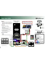
Schematic diagram
Summary of Contents for KA05
Page 3: ...Velleman N V Legen Heirweg 33 9890 Gavere België ...
Page 10: ... 10 PCB ...