© 2009 UTC RETAIL
11
11692017 Rev
A
6. Raise the cover
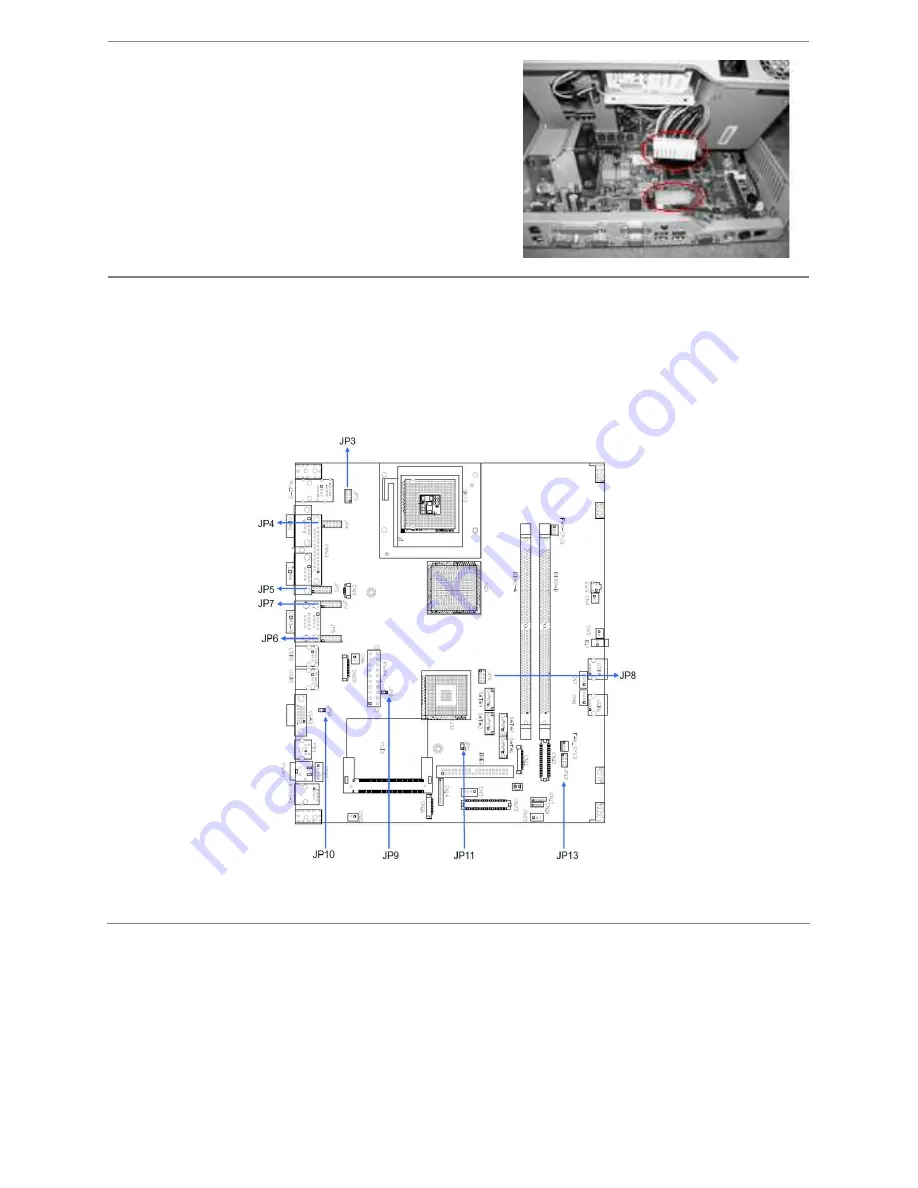
Pivot the cover up; unplug the power connector (circled in red in
the photo to the right) by pressing its tab and pulling it out of the
motherboard jack. Raise the cover fully; aligning the pivot screws
in the chassis slots and locking the rear cover up at a 45° angle.
7. Configure the COM port to p5VDC to Pin 9
Use the drawing below to locate the terminal block you need. COM1
→
JP4, COM2
→
JP5, COM3
→
JP7, COM4
→
JP6.
The drawing’s left side is the rear of the motherboard; pin 1 on each terminal block is indicated by the small black
circle. When pins 7 and 8 are jumpered, pin 9 of the serial port is signal RI for a modem. When pins 9 and 10 are
jumpered, +5VDC is routed to pin 9 of the serial port. Remove the jumper connecting pins 7 and 8 and install it to
connect pins 9 and 10. On a 3100 Series in its standard configuration, JP4 has a jumper connecting pins 7 and 8,
whereas on JP5, JP7 and JP6 that jumper has been moved to connect pins 9 and 10.
Reverse previous steps to close the cover. Lift the chassis cover out of the locking slots, reconnect the power cable,
lay the cover flat on the main chassis and slide it forward the half inch required to seat the pivot barrels into their
mating slots.


