background image

7

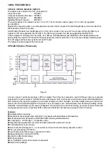
31. Scart input 1 in, left

50. Scart output 2, left

32. Analog Shield Ground 1

51. Scart output 2, right

33. Scart input 2 in, right

52. Analog Shield Ground 3

34. Scart input 2 in, left

53. Not connected

35. Analog Shield Ground 2

54. Not connected

36. Scart input 3 in, right

55. Not connected

37. Scart input 3 in, left

56. Analog output Channel 1, left

38. Analog Shield Ground 4

57. Analog output Channel 1, right

39. Not connected

58. Reference ground 2 high voltage part

40. Not connected

59. Analog output Channel 2, left

41. Not connected

60. Analog output Channel 2, right

42. Analog reference voltage high voltage part

61. Power-on-reset

43. Analog ground

62. Not connected

44. Volume capacitor Channel1

63. Not connected

45. Analog power supply 8.0 V

64. I2S2-data output

46. Volume capacitor Channel 2

65. I2S2-data input

47. Scart output 1, left

66. Digital ground

48. Scart output 1, right

67. Digital power 5 V

49. Reference ground 1 high voltage part

68. Not connected

HEADPHONE  OUTPUT

TDA1308

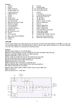
The TDA1308 is an integrated class AB stereo headphone driver. It gets its input from two analog audio outputs (DACA_L

and DACA_R) of MSP3410D. The gain of the output is adjustable by the feedback resistor between the inputs and outputs.

Features:

n

Wide temperature range

n

No switch ON/OFF clicks

n

Excellent power supply ripple rejection

n

Low power consumption

n

Short-circuit resistant

n

High performance

- high signal-to-noise ratio

- high slew rate

- low distortion

n

Large output voltage swing

Pinning:

1. Output A (Voltage swing) : Min : 0.75V, Max : 4.25V

2. Inverting input A

: Vo(clip) : Min : 1400mVrms

3. Non-inverting input A

: 2.5V

4. Ground

5. Non-inverting input B

: 2.5V

6. Inverting input B

: Vo(clip) : Min : 1400mVrms

7. Output B (Voltage swing) : Min : 0.75V, Max : 4.25V

8. Positive supply

: 5V, Min : 3.0V, Max : 7.0V

AUDIO OUTPUT

TDA7265

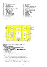
The TDA7265 is a 25W+25W stereo sound amplifier with mute/stand-by facility. STPA control signal coming from microcontroller

(when it is at high level) activates the mute function. IC is muted when mute port is at low level. Two stereo audio signals

coming from audio module is injected to the inputs of the IC and a power of 12Wrms (10%) is obtained. An external pop-

noise circuitry pulls AF inputs of the IC in order to eliminate pop noise when TV is turned on or off via mains supply

connection. It is possible to adjust the gain of the amplifiers by feedback external resistors.

Features:

n

Wide supply voltage range (up to 50V ABS Max.)

n

Split supply

n

High output power: 25+25 W @ TDA = 10%, RL = 8ohm, VS = ±20V

n

No pop at turn-on / off

n

Mute (pop free)

n

Stand-By feature (low IQ)

n

Few external components

n

Thermal overload protection

n

Adjustable gain via an external resistor

Summary of Contents for FT-81015

Page 1: ...SERVICE MANUAL UNIVERSUM FT 81015 MODEL ...

Page 2: ...CIP3250 13 14 SDA9400 14 15 DDP3310 15 16 AK28 CHASSIS MANUALADJUSTMENTS PROCEDURE 17 PRELIMINARY 17 SYSTEM VOLTAGEAJUSTMENT 17 AFCADJUSTMENT 17 FOCUSADJUSTMENT 17 SCREENADJUSTMENT 17 IFADJUSTMENT FOR L MODE 17 AK28 CHASSIS PRODUCTION MODE ADJUSTMENTS PROCEDURE 18 PRELIMINARY 18 HORIZONTALAND VERTICALGEOMETRY ALIGNMENTS 18 V SHIFT 18 V SIZE 18 H SHIFT 18 H SIZE 18 S COR 18 LINRT 18 ANGLE 18 BOW 18...

Page 3: ...Ground Blue 6 Audio left input 0 5Vrms 10K 6 Audio left input 0 5Vrms 10K 7 Blue input 0 7Vpp 75ohm 7 Blue input 0 7Vpp 75ohm 8 AV switching input 0 12VDC 10K 8 AV switching input 0 12VDC 10K 9 Ground Green 9 Ground Green 10 10 11 Green input 0 7Vpp 75ohm 11 12 12 13 Ground Red 13 Ground Red 14 Ground Blanking 14 Ground Blanking 15 Red input 0 7Vpp 75ohm 15 16 Blanking input 0 0 4VDC 1 3VDC 75ohm ...

Page 4: ... n Synchronization and Fixed Frequency Facility n Over and Under voltage Lockout n Switch Off at Mains Under voltage n Mains Voltage Dependent Fold Back Point Correction n Low Power Consumption n Free usable Fault Comparators Pinning 1 OTC Off Time Circuit 2 PCS Primary Current Simulation 3 RZI Regulation and Zero Crossing Input 4 SRC Soft Start and Regulation Capacitor 5 OCI Opto Coupler Input 6 ...

Page 5: ...r AGC current 2mA 11 Available tuner AGC current Min 0 3V Max 13 5V 12 Video output Min 1 8V Max 2 2V 13 Standard switch Min 0V Max 0 8V 14 L switch Min 0V Max 3 0V 15 IF gain control range 65dB 16 Ground 17 Internal reference voltage 18 FPLL and VCO Min 1mA Max 4mA 19 AFC switch Min 0V Max 0 8V 20 FPLL and VCO Min 1mA Max 4mA 21 FPLL and VCO Min 1mA Max 4mA 22 AFC output 0 7 mA kHz 23 DC supplay ...

Page 6: ... necessary for tuning the open loop frequency of the internal PLL and for stabilising the frequency in closed loop operation The higher the capacitors the lower the clock frequency result The nominal free running frequency should match the centre of the tolerance range between 18 433 and 18 431Mhz as closely as possible By means of standardised I2S interface additional feature processors DPL35xx D...

Page 7: ...rt input 1 in left 65 I S2 data input 32 Analog Shield Ground 2 66 Digital ground 33 Scart input 2 in right 67 Digital power supply 5V 34 Scart input 2 in left 68 ADR clock DOLBY PRO LOGIC PROCESSOR IC DPL3519A The IC DPL3519A processor family is designed to decode Dolby encoded surround sound The IC integrate the complete Dolby Surround Pro Logic decoding on chip without any necessary external ci...

Page 8: ...s n Wide temperature range n No switch ON OFF clicks n Excellent power supply ripple rejection n Low power consumption n Short circuit resistant n High performance high signal to noise ratio high slew rate low distortion n Large output voltage swing Pinning 1 OutputA Voltage swing Min 0 75V Max 4 25V 2 Inverting inputA Vo clip Min 1400mVrms 3 Non inverting inputA 2 5V 4 Ground 5 Non inverting inpu...

Page 9: ...ax 3mA 9 Vcc 12V 10 Input Max 2Vpp Input Current 1mA Max 3mA 11 Input Max 2Vpp Input Current 1mA Max 3mA 12 Ground 13 Output 5 5Vpp Min 4 5Vpp 14 Output 5 5Vpp Min 4 5Vpp 15 Output 5 5Vpp Min 4 5Vpp 16 Output 5 5Vpp Min 4 5Vpp 17 Output 5 5Vpp Min 4 5Vpp 18 Output 5 5Vpp Min 4 5Vpp 19 Ground 20 Input Max 2Vpp Input Current 1mA Max 3mA VIDEO OUTPUT AMPLIFIER STAGE TDA6111Q The TDA6111Q is a video o...

Page 10: ...chitecture and instruction set are based upon that of the 8051 microcomputer Like the 8051 has many features which increase programming ease extended internal data memory space variable manipulation in internal data memory free stack location in data RAM 4 register banks special function registers memory mapped I O individually addressable bits and a Boolean processor give the programmer the abili...

Page 11: ...nstruction cycle at 12 MHz internal clock rate 8 data pointer registers n Serial interface Full duplex UART interface I C compatible interface SDA 30C264 only n On Chip RAM Direct byte and bit addressability Four register banks 256 bytes of data memory including 128 user defined software flags 2048 bytes of data memory accessible with MOVX instructions SDA 30C263 1024 bytes n External Program Memo...

Page 12: ...ersion n Output unlatched at cycle and allows two dimensional chip selection n Read writes read modify write CAS before RAS refreshes RAS only refresh hidden refresh and test mode capability n All inputs and outputs TTL compatible n 1024 refresh cycles 16 ms n 1024 refresh cycles 128 ms Low Power Version only n Plastic Packages P SOJ 26 20 5 with 300mil width EPROM ST27C2001 The ST27C2001 is 2097 ...

Page 13: ...IC has four composite one SVHS input and one composite output which is used for teletext InAK28 the main video input is Vin2 which is also used for luma input in SVHS applications After switching the inputs the signals are converted to digital via two 8 bit ADCs And these digital data are processed to produce the 4 2 2 formatted digital YUV signals The main features are multi standard color decodi...

Page 14: ...Top Analog 34 Ground CIP3250 The IC is used to interface the analog input which is output from the PIP module SCART RGB or PIP RGB As can be seen from the block diagram there is a CT BR SAT block which is used for luma contrast brightness hue and color saturation correction The soft mixer is controlled by the fast blank signal Features n analog input for RGB or YUV and Fast Blank n triple 8 bit an...

Page 15: ...Voltage 5 V SDA9400 SDA9400 converts the scan rate from 50 60 Hz to 100 120 Hz Features Two input data formats 4 2 2 luminance and chrominance parallel 2 x 8 wires ITU R 656 data format 8 wires Two different representations of input chrominance data 2 s complement code Positive dual code Flexible input sync controller Flexible compression of the input signal Digital vertical compression of the inp...

Page 16: ...ster External synchronization by backend IC possible e g split screen for one TV channel with joint lines and one PC VGA channel Signal manipulations Insertion of coloured background Vertical and or horizontal windowing with four different speed factors Flash generation for supervising applications motion flag readable by I C bus Still frame or field Support of split screen applications Multiple p...

Page 17: ...ncy doubling two I2C controlled PWM outputs beam current limiter Pinning 1 Supply Voltage 28 Sup Volt Analog Back end 2 Gnd Output Pin Driver 29 VRD BCS DAC Ref Beam Current Safety 3 Additional VSYNC input 30 Fast Blank1 Input 4 Read counter Reset 31 Analog Red1 Input 5 FIFO Read Enable 32 Analog Green1 Input 6 FIFO Write Enable 33 Analog Blue1 Input 7 FIFO Write counter Reset 34 Fast Blank2 Input...

Page 18: ...lts TV should automatically tune to a station when search tuning is activated D FOCUS ADJUSTMENT Inputs AC power PAL B G test pattern via RF input Outputs Picture tube drive Display Picture Action Select TV mode and tune to the signal Adjust focus potentiometer the upper pot on the rear side of the FBT transformer for optimum focusing drive E SCREEN ADJUSTMENT Inputs AC power PAL B G Colour Bar te...

Page 19: ...est pattern is horizontally in equal distance both to right and left sides of the picture tube Check and readjust H SHIFT item if the adjustment becomes improper after some other geometric adjustments are done 4 H SIZE Adjust H WIDTH item by pressing cursor left and or cursor right buttons till no under scan condition will happen i e no white bars on the left and right side of the test pattern wil...

Page 20: ...d BGn by cursor up and or cursor down buttons and change the values by cursor left and or cursor right buttons till the following values are read X 285 10 Y 293 10 on the colour analyser 2 RRf GRf BRf Set the values of these items as 62 constant 3 YDF Apply COLOUR BAR test pattern Select YDF item cursor up and or cursor down buttons Adjust YDF by pressing cursor left and or cursor right buttons ti...

Page 21: ...of the PIP frame edges of the PIP EHTHP EHT compensation coefficient for horizontal phase EHTHTC EHT time contant for horizontal phase compensation EHTH EHT compensation coefficient for horizontal amplitude EHTV EHT compensation coefficient for vertical amplitude EHTV TC time contant for control of vertical and horizontal amplitude EHT compenzation 0 means off OSD LEVEL contast level of the OSD IN...

Page 22: ... 2 0 2 8 0 2 B 6 8 6 1 1 B 1 7 9 2 7 5 9 9 9 9 9 B 6 7 7 7 7 5 7 2 5 9 5 7 6 7 96 6 9 6 6 2 6 5 5 B 2 8 7 6 9 0 0 8 7 3 5 2 7 6 9 6 8 6 5 6 6 6 7 H U U H V W H U L D O 7 X Q H U F W L Y H 6 S O L W W H U 7 0 6 3 3 9 3 3 6 3 3 3 7 X Q H U 6 6 6 5 6 7 9 5 6 5 6 5 6 6 2 8 1 2 5 1 9 6 7 1 2 5 7 9 L G H R 6 Z L W F K L Q J 0 D W U L 6 5 7 6 5 7 6 5 7 0 6 3 D F N B 9 U R Q W B 9 6 6 6 6 6 6 0 2 1 2 1 4 ...

Page 23: ...BLE WITH 11DS28Q 4 MODUL MODIFICATION TO IMPROVE DEEP NOISE ON PCB 11DS28Q 4 CONNECT A CABLE BETWEEN GROUND OF C579 NEAR TO IC 501 AND GROUND OF C556 NO PCB CODE VESTEL CODE COMPONENT NAME POSITION NUMBER QUANTITY 1 30014955 PCB 11DS28Q 4 1 2 3 4 5 IN NO PCB CODE VESTEL CODE COMPONENT NAME POSITION NUMBER QUANTITY 1 30016811 PCB 11DS28Q 7 1 2 3 4 5 CUSTOMER SUPPORT ENGINEER QUALITY MANAGER S DEMIR...

Page 24: ...074 CAP MKT 100NF 63V J C 202 1 4 11 AK 28 10 30000315 CAP SMD 220NF 25V Z 0805 C 203 1 5 11 AK 28 10 DVD Lİ 30008766 OPTIC AUDIO OUTPUT TOTX176 JK 001 1 6 11 AK 28 10 DVD Lİ 30000818 RES SMD 1 10W 8 2K J 0805 R 519 1 7 8 9 10 COMPONENTS IN No PCB Code Pic No VESTEL Code Description Position Amount 1 30017572 PCB 11AK28 10 1 2 11 AK 28 10 30006743 TRF HORIZONTAL DRIVER 15AK17 17 TR 201 1 3 11 AK 2...

Page 25: ...8766 OPTIC AUDIO OUTPUT TOTX176 JK 001 1 6 11 AK 28 10 DVD Lİ 30000818 RES SMD 1 10W 8 2K J 0805 R 519 1 7 8 9 10 COMPONENTS IN No PCB Code Pic No VESTEL Code Description Position Amount 1 30017572 PCB 11AK28 10 1 2 11 AK 28 10 30006743 TRF HORIZONTAL DRIVER 15AK17 17 TR 201 1 3 11 AK 28 10 30000106 CAP MKT 47NF 100V J C 202 1 4 11 AK 28 10 30000099 CAP MKT 33NF 63V J C 203 1 5 11 AK 28 10 3000197...

Page 26: ... 901 SP XX 2 4 11 TP 28 VER 5 30000580 RES CF 1 4W 22R J R 940 1 5 11 TP 28 VER 5 30001994 FIXED COIL 22UH J AXIAL J 921 1 6 11 TP 28 VER 5 30002583 KISA DEVRE TELİ 0 6MM J 920 1 7 11 TP 28 VER 5 30000295 CAP CER 100NF 50V Z F C 940 1 8 11 TP 28 VER 5 30002876 CABLE ASSY 1 25 AK19 EMC 1 9 10 COMPONENTS IN No PCB Code Pic No VESTEL Code Description Position Amount 1 30017573 PCB 11TP28 7 1 2 11 TP ...

Page 27: ...d to this bulletin E Others SUBJECT C216 defect DATE April 05 2002 Objective Please modify if following symptom occurs Symptom TV does not work due to C216 broke down Cause Because of overheating on C216 Countermeasures In order to decrease temperature on C216 modify the chassis as given below Replace C216 EL CAP 4 7 UF 250V 85ºC EL CAP 47 UF 250V 105ºC High Ripple Spare Parts order C216 VE 300004...

Page 28: ...074 CAP MKT 100NF 63V J C 202 1 4 11 AK 28 10 30000315 CAP SMD 220NF 25V Z 0805 C 203 1 5 11 AK 28 10 DVD LI 30008766 OPTIC AUDIO OUTPUT TOTX176 JK 001 1 6 11 AK 28 10 DVD LI 30000818 RES SMD 1 10W 8 2K J 0805 R 519 1 7 8 9 10 COMPONENTS IN No PCB Code Pic No VESTEL Code Description Position Amount 1 30017572 PCB 11AK28 10 1 2 11 AK 28 10 30006743 TRF HORIZONTAL DRIVER 15AK17 17 TR 201 1 3 11 AK 2...

Page 29: ...8766 OPTIC AUDIO OUTPUT TOTX176 JK 001 1 6 11 AK 28 10 DVD LI 30000818 RES SMD 1 10W 8 2K J 0805 R 519 1 7 8 9 10 COMPONENTS IN No PCB Code Pic No VESTEL Code Description Position Amount 1 30017572 PCB 11AK28 10 1 2 11 AK 28 10 30006743 TRF HORIZONTAL DRIVER 15AK17 17 TR 201 1 3 11 AK 28 10 30000106 CAP MKT 47NF 100V J C 202 1 4 11 AK 28 10 30000099 CAP MKT 33NF 63V J C 203 1 5 11 AK 28 10 3000197...

Page 30: ... 901 SP XX 2 4 11 TP 28 VER 5 30000580 RES CF 1 4W 22R J R 940 1 5 11 TP 28 VER 5 30001994 FIXED COIL 22UH J AXIAL J 921 1 6 11 TP 28 VER 5 30002583 KISA DEVRE TELI 0 6MM J 920 1 7 11 TP 28 VER 5 30000295 CAP CER 100NF 50V Z F C 940 1 8 11 TP 28 VER 5 30002876 CABLE ASSY 1 25 AK19 EMC 1 9 10 COMPONENTS IN No PCB Code Pic No VESTEL Code Description Position Amount 1 30017573 PCB 11TP28 7 1 2 11 TP ...

Page 31: ... MODUL IS COMPATIBLE WITH 11DS28Q 4 MODUL MODIFICATION TO IMPROVE DEEP NOISE ON PCB 11DS28Q 4 CONNECT A CABLE BETWEEN GROUND OF C579 NEAR TO IC 501 AND GROUND OF C556 NO PCB CODE VESTEL CODE COMPONENT NAME POSITION NUMBER QUANTITY 1 30014955 PCB 11DS28Q 4 1 2 3 4 5 IN NO PCB CODE VESTEL CODE COMPONENT NAME POSITION NUMBER QUANTITY 1 30016811 PCB 11DS28Q 7 1 2 3 4 5 CUSTOMER SUPPORT ENGINEER QUALIT...

Page 32: ...ptom TV does not sense to R C signals in the standard distance Cause The gain tolerance of IR receivers Countermeasures In order to improve to R C sensitivity distance modify the touch board function buttons card as given below Connect a CAP EL 22UF 50V M between the middle pin and the 1st pin Ground of IR receiver Please solder the point of 22uF capacitor to the middle pin of IR receiver Solder p...

Page 33: ......

Page 34: ......

Page 35: ......

Reviews: