3
POWER SUPPLY (SMPS)
TDA16846
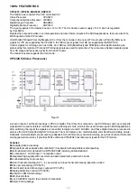
A SMPS transformer controlled by the IC TDA16846, which is designed for driving, controlling, and protecting switching
transistor, provides the DC voltages required at various parts of the chassis. SMPS generates the necessary 5V supply for
the micro-controller, 130V supply for the FBT, +/-16V supply for the audio amplifier, which are active in stand-by and others
8V, 12V and 5V for other different parts of the chassis.
When the TV is switched on, a reference voltage is provided to TDA16846 and the start-up operation occurs, then TV enters
into the stand-by position.
Two optocouplers are used to control the regulation of line voltage and stand-by power consumption. There are two regulation
circuits, one in primary side and one in secondary side. The primary regulation circuit provides a control voltage to pin3 of the
IC. Secondary regulation circuit produces a control voltage according to the changes in 130V DC voltage, via an optocoupler
(SFH617A) to pin4 of the IC.
During the switch on period of the transistor, energy is stored in the transformer. During the switch off period energy is fed to
the load via secondary winding. By varying switch-on time of the power transistor, it controls each portion of energy transferred
to the second side such that the output voltage remains nearly independent of load variations. At the same time, the supply
voltages 12V, 8V, 5V are stabilised by the series regulators.
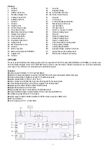
Features:
n
Line Current Consumption with PFC
n
Continuous Frequency Reduction with Decreasing Load
n
Stable and Adjustable Stand-by Frequency
n
Very Low Start-up Current
n
Soft-Start for Quiet Start-up
n
Adjustable and Voltage Dependent Ringing Suppression Time
n
Synchronization and Fixed Frequency Facility
n
Over- and Under-voltage Lockout
n
Switch Off at Mains Under-voltage
n
Mains Voltage Dependent Fold Back Point Correction
n
Low Power Consumption
n
Free usable Fault Comparators
Pinning:
1. OTC Off Time Circuit
2. PCS Primary Current Simulation
3. RZI
Regulation and Zero Crossing Input
4. SRC Soft-Start and Regulation Capacitor
5. OCI Opto Coupler Input
6. FC2 Fault Comparator 2
7. SYN Synchronization Input
8. N. C. Not Connected
9. REF Reference Voltage and Current
10. FC1 Fault Comparator 1
11. PVC Primary Voltage Check
12. GND Ground
13. OUT Output
14. VCC Supply Voltage
IF PART
TDA4470 / TDA4472
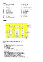
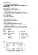
The TDA44XX is an integrated bipolar circuit for multistandard video/sound IF (VIF/SIF) signal processing in TV/VCR and
multimedia applications. The circuit processes all TV video IF signals with negative modulation (e.g., B/G standard), positive
modulation (e.g., L standard) and the AM, FM/NICAM sound IF signals. Active carrier generation by FPLL (frequency phase-
locked loop) is the principle for true synchronous demodulation. VCO circuit is operating on picture carrier frequency, the
VCO frequency is switchable for L´-mode. AFC without external reference circuit is alignment-free and polarity of the AFC
curve is switchable. VIF-AGC for negative modulated signals operates on peak sync detection principle and for positive
modulation on peak white / black level detection principle. Tuner AGC is adjustable with determining take over point. It has
alignment-free quasi-parallel sound (QPS) mixer for FM/NICAM sound IF signals. Intercarrier output sound is gain controlled
(necessary for digital sound processing). AM-demodulator is completely alignment-free with gain controlled AF output.
Operation of the AM demodulator and QPS mixer (for NICAM-L stereo sound is parallel. TDA4472 is used for negative
modulation and TDA4470 is used for both negative and positive modulation.
Summary of Contents for FT-81015
Page 1: ...SERVICE MANUAL UNIVERSUM FT 81015 MODEL ...
Page 33: ......
Page 34: ......
Page 35: ......


