SARA-R42 - Application note
UBX-20050829 - R02
Testing
Page 41 of 58
C1-Public
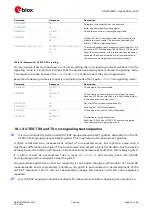
Command
Response
Description
AT+COPS=2
OK
Deregister the module from the network.
AT+UTEST=1
OK
Enter the non-signaling mode again.
AT+UTEST?
+UTEST: 1
OK
Check the module is in non-signaling mode.
AT+CFUN?
+CFUN: 5
OK
Check +CFUN AT command is set to 5 to ensure the
module is in test mode. The device is now ready for
either TX, RX non-signaling tests.
AT+UTEST=2,101575,1500
+UTEST: 101575,1500,0,-70,-
70,-70
OK
The module measures the receiver power level for 1.5 s
at channel 1575 (frequency 1842.50 MHz LTE band 3).
After the time interval, the information text response
contains: the channel number, the time interval and
the minimum, average, maximum power levels.
Table 14: Example of +UTEST RF Rx testing
For any module (factory brand-new or not) when exiting the non-signaling mode to get back into the
signaling mode, it is important to check that the device has properly been restored to signaling mode.
This requires a check between the
+UTEST
and
+CFUN
state to see if they are in agreement.
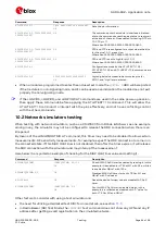
Example of checking module is properly in signaling mode after it exits
+UTEST
non-signaling mode:
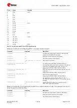
Command
Response
Description
AT+UTEST?
+UTEST: 0
OK
The device is in normal mode.
AT+CFUN?
+CFUN: 5
OK
The device is not completely in non-signaling mode
bCFUN reports that it is in test mode. Below
is the sequence to correct this.
AT+CFUN=0
OK
Set the MT to minimum functionality.
AT+CFUN=1
OK
Sets the MT to full functionality.
AT+CFUN?
+CFUN: 1
OK
The device is now set to full functionality.
AT+UTEST?
+UTEST: 0
OK
The device is in signaling mode.
Both the +CFUN and +UTEST AT commands agree
that the device is in signaling mode.
10.1.3
UTEST RX and TX non-signaling test sequence
☞
It is recommended to perform all RX UTEST grouped sequentially together, separate from the TX
UTESTs test grouped sequentially together. This may help avoid measurement glitches.
A glitch is defined as a measurement output of an expected value, but reports a value with a
significant differential. Example: if the module were instructed to transmit 20 dBm, but the device
actually transmits 0 dBm, and there is no RF connectivity hardware at fault, then this is likely a glitch.
If a glitch should be encountered then a reset (
AT+CFUN=15
) and re-entry back into UTEST
non-signaling mode is required to clear the glitch.
A measurement glitch does not occur randomly; it can happen through a combination of TX and RX
measurements and is reproducible. Therefore, if a glitch is encountered in the development of the
+UTEST sequence, then it will not unexpectedly change the behavior with the same sequence
repeated.
☞
Any +UTEST sequence should be verified with measurements before deploying into production.


