


25
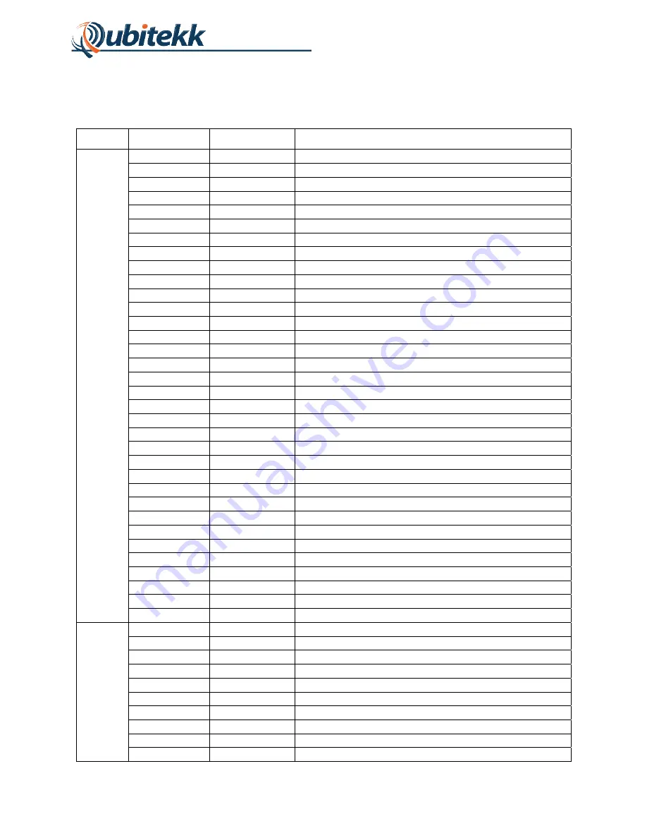
A.3 Pinout Table
The pinout table for the RCM3400 is shown below:
Header
Pin Number
Pin Name
Description
J1
1 LN3
Not
Connected
2 LN7
Not
Connected
3 LN2
Not
Connected
4 LN6
Not
Connected
5 LN1
Not
Connected
6 LN5
Not
Connected
7 LN0
Not
Connected
8 LN8
Not
Connected
9 VREF
Not
Connected
10 CONVERT
Not
Connected
11
PF6
Coincidence Window or Delay (Bit 2)
12
PF7
Bus to LCD Display (Line E)
13
PF4
Bus to FPGA Counter (Bit 7)
14
PF5
Bus to FPGA Counter (Overflow Flag)
15
PB7
Bus to FPGA Counter (Bit 21)
16
PE7
Bus to LCD Display (Line RS)
17
PE6
Start/Stop Button on User Interface
18
PE5
Down Button on User Interface
19
PE4
Bus to LCD Display (Line 4)
20
PE2
Clear Button on User Interface
21
PE1
Bus to LCD Display (Line 5)
22
PE0
Menu Button on User Interface
23 GND
Ground
24
+3_3V_IN
+3.3V Input (Power)
25
PG7
Bus to LCD Display (Line 6)
26
PG6
Enable/Select Button on User Interface
27
PG5
Bus to LCD Display (Line 7)
28
PG4
Up Button on User Interface
29 /IORD
Not
Connected
30
STATUS
Reserved for firmware upload
31
SMODE1
Reserved for firmware upload
32 /IOWR
Not
Connected
33
/RES
Reserved for firmware upload
34
SMODE0
Reserved for firmware upload
J2
1 GND
Ground
2
PF1
Coincidence Window or Delay (Bit 0)
3
PB6
Bus to FPGA Counter (Bit 0)
4
PF0
Bus to FPGA Counter (Bit 14)
5
PB5
Bus to FPGA Counter (Bit 1)
6
PB4
Bus to FPGA Counter (Bit 15)
7
PB3
Bus to FPGA Counter (Bit 2)
8
PB2
Bus to FPGA Counter (Bit 16)
9
PB1
Reserved for firmware upload
10
PA7
Bus to FPGA Counter (Bit 17)
Summary of Contents for CC1
Page 1: ...CC1 Handheld Coincidence Counter USER S MANUAL Rev 1 02 June 1 2015 www qubitekk com...
Page 7: ...4 Figure 4 CC1 Buttons and Ports...
Page 23: ...20 APPENDIX A Electrical Schematics and Connections...
Page 24: ...21 A 1 Top Board LCD Display...
Page 25: ...22 A 2 Bottom Board FPGA and Microprocessor...
Page 26: ...23...
Page 27: ...24...


