


LARA-R2 series - System Integration Manual
UBX-16010573 - R02
Objective Specification
Design-in
Page 77 of 148
2.2.1.10
Guidelines for removing VCC supply
As described in section 1.6.2 and Figure 14, the
VCC
supply can be removed after the end of LARA-R2 series
modules internal power-off sequence, which has to be properly started sending the AT+CPWROFF command
(see
u-blox AT Commands Manual
[2]).
Removing the
VCC
power can be useful in order to minimize the current consumption when the LARA-R2 series
modules are switched off. Then, the modules can be switched on again by re-applying the
VCC
supply.
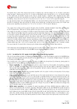
If the
VCC
supply is generated by a switching or an LDO regulator, the application processor may control the
input pin of the regulator which is provided to enable / disable the output of the regulator (as for example the
RUN input pin for the regulator described in Figure 26, the INH input pin for the regulator described in Figure 27,
the SHDNn input pin for the regulator described in Figure 28, the EN input pin for the regulator described in
Figure 29), in order to apply / remove the
VCC
supply.
If the regulator that generates the
VCC
supply does not provide an on / off pin, or for other applications such as
the battery-powered ones, the
VCC
supply can be switched off using an appropriate external p-channel MOSFET
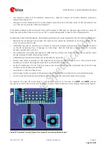
controlled by the application processor by means of a proper inverting transistor as shown in Figure 35, given
that the external p-channel MOSFET has provide:
Very low R
DS(ON)
(for example, less than 50 m
), to minimize voltage drops
Adequate maximum Drain current (see
LARA-R2 series
[1] for module consumption figures)
Low leakage current, to minimize the current consumption
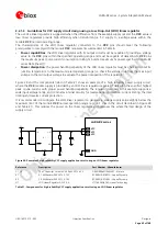
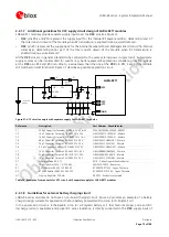
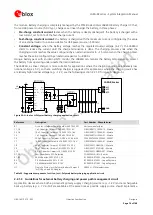
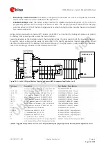
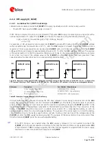
C3
GND
C2
C1
C4
LARA-R2 series
52
VCC
53
VCC
51
VCC
+
VCC Supply Source
GND
GPIO
C5 C6
R1
R3
R2
T2
T1
Application
Processor
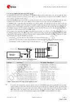
Figure 35: Example of application circuit for VCC supply removal
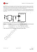
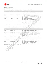
Reference
Description
Part Number - Manufacturer
R1
47 k
Resistor 0402 5% 0.1 W
RC0402JR-0747KL - Yageo Phycomp
R2
10 k
Resistor 0402 5% 0.1 W
RC0402JR-0710KL - Yageo Phycomp
R3
100 k
Resistor 0402 5% 0.1 W
RC0402JR-07100KL - Yageo Phycomp
T1
P-Channel MOSFET Low On-Resistance
AO3415 - Alpha & Omega Semiconductor Inc.
T2
NPN BJT Transistor
BC847 - Infineon
C1
330 µF Capacitor Tantalum D_SIZE 6.3 V 45 m
T520D337M006ATE045 - KEMET
C2
10 nF Capacitor Ceramic X7R 0402 10% 16 V
GRM155R71C103KA01 - Murata
C3
100 nF Capacitor Ceramic X7R 0402 10% 16 V
GRM155R61A104KA01 - Murata
C4
56 pF Capacitor Ceramic C0G 0402 5% 25 V
GRM1555C1E560JA01 - Murata
C5
15 pF Capacitor Ceramic C0G 0402 5% 25 V
GRM1555C1E150JA01 - Murata
C6
8.2 pF Capacitor Ceramic C0G 0402 5% 50 V
GRM1555C1H8R2DZ01 - Murata
Table 27: Components for VCC supply removal application circuit
It is highly recommended to avoid an abrupt removal of the
VCC
supply during LARA-R2 series modules
normal operations: the power off procedure must be started by the AT+CPWROFF command, waiting the
command response for a proper time period (see
u-blox AT Commands Manual
[2]), and then a proper
VCC
supply has to be held at least until the end of the modules’ internal power off sequence, which
occurs when the generic digital interfaces supply output (
V_INT
) is switched off by the module.


