GPS Receiver A1030-A
5.1.2 Description
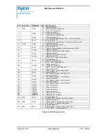
This table describes the functionality of the pins with Tyco Standard GPS firmware
or Dead Reckoning firmware running on the module. The associated symbols are
explained. General-purpose pins that are not supported in the standard firmware
are explained further down below.
Pin Symbol
Description
1
GND
Ground (power supply)
3
Vcc
+3.3V (power supply)
5
VBAT
Back-up battery supply pin (RTC and SRAM)
7
ENABLE
Enable pin – low power when low
9 nRST
Reset
input
11
Rx0
Serial input 0, NMEA in
13
Tx0
Serial output 0, NMEA out
19
Rx2
Serial input 2, RTCM input (DGPS)
21
Tx2
Serial output 2
23
TEST0
Reserved for test purposes
29
Vgyro
Input pin for gyro output voltage (required for DR)
33
LOCK
Activated on LOCK (position fix)
37
GS
Gain Select for LNA – leave open
39
ANTSTAT
Antenna sensor output
41
VANT
Power supply Antenna external
45
Vcc3A
Analog voltage supply < +3.3V (required for DR)
47
Odo
Odometer input (required for DR)
49
F/R
Reverse signal input (required for DR)
Table 4: Pin out description (odd signal numbers)
Pin Symbol
Description
2
Res.
Reserved for future use – do not connect
10
1PPS
1PPS (pulse per second) output
46
Res.
Reserved for future use – do not connect
48
Res.
Reserved for future use – do not connect
50
Res.
Reserved for future use – do not connect
Table 5: Pin out description (even signal numbers)
V2.0 - 07/05
User’s Manual
Page 15 of 37


