background image

Hangzhou Tuya Inc.

NM1 Module Hardware Design Manual

https://www.tuya.com

Page 28 of 29

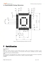
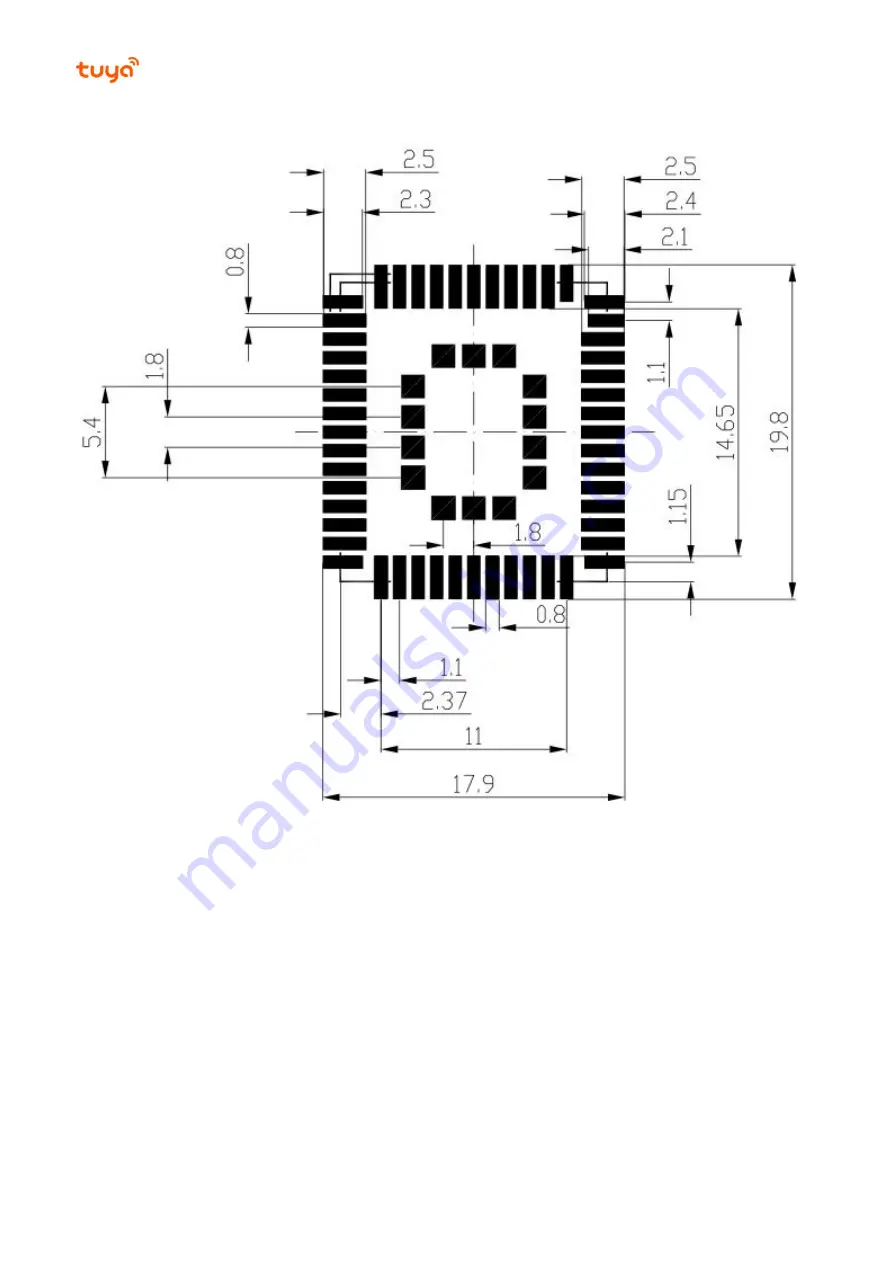
6.2 Recommended Package Dimensions

Figure 6- 4 Recommended package dimensions (unit: mm)

7

Certification

FCC Statement

15.19

This device complies with Part 15 of the FCC Rules. Operation is subject to the following two conditions: (1) This

device may not cause harmful interference. (2) This device must accept any interference received, including

interference that may cause undesired operation.

15.21

Note: The grantee is not responsible for any changes or modifications not expressly approved by the party responsible

for compliance. Such modifications could void the user’s authority to operate the equipment.

15.105(b

)

Summary of Contents for NB-IoT Series

Page 1: ...in stores Its solutions cover hardware access cloud services and app software development forming a closed service loop of AI and manufacturing It provides business group technologies and business mod...

Page 2: ...odule Hardware Design Manual https www tuya com Page 2 of 29 Change History Date Version Change Description Prepared By Reviewed By Approved By 2019 03 01 1 0 This is the first release Wang Yanfeng Wa...

Page 3: ...resentations of any kind either express or implied for content in this document and is not reliable for specific merchantability applicability and indirect special or associated losses Confidentiality...

Page 4: ...6 1 Pins 17 3 6 2 I2 C Interface Electrical Parameters and Application 18 3 7 UART Interface 18 3 7 1 Pins 18 3 7 2 UART Interface Electrical Parameters and Application 18 3 8 USB Interface 19 3 8 1...

Page 5: ...lculation data 23 Figure 5 1 Recommended stencil strips 24 Figure 5 2 Over temperature curve 25 Figure 6 1 Top view unit mm 26 Figure 6 2 Side view unit mm 26 Figure 6 3 Transparent view unit mm 27 Fi...

Page 6: ...nd technical parameters this document also describes the product reliability test related test standards service function implementation process RF performance indicators and circuit design 1 3 Refere...

Page 7: ...le It has the following features Supports the B1 B3 B5 B8 B20 frequency bands Provides the SIM card interface 1 8 V USB 1 1 interface UART interface SPI I2 C interface and GPIO interface Figure 2 1 Pr...

Page 8: ...e is disconnected from the network and cannot receive paging messages The NM1 module is woken up from the PSM mode when the timer expires or the PWRKEY and PSM_EINT pins are lowered Power saving In PS...

Page 9: ...us indicator signal module startup and reset signals and multiplexing control signals power supply and grounding of multiple GPIO interfaces Figure 2 3 System connection framework 2 3 2 RF Functions T...

Page 10: ...input power W 50 Input impedance ohm 50 Polarization type Linear polarization Note The NM1 module is being developed to support the frequency bands with an asterisk Table 2 5 Conducted RF transmit po...

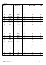
Page 11: ...ls 3 1 2 Pin Configuration Diagram Figure 3 1 shows the NM1 module s interface pins Figure 3 1 Pin configuration diagram 3 1 3 Pins Table 3 2 Interface pin definition Pin No Analog Signal Definition P...

Page 12: ...A N A N A 11 SIM_DATA SIM card data signal I O Maximum value of VIL 0 25 x SIM_VDD Minimum value of VIH 0 75 x SIM_VDD Maximum value of VOL 0 15 x SIM_VDD Minimum value of VOH 0 85 x SIM_VDD N A 12 S...

Page 13: ...T1_TXD Auxiliary serial interface that transmits data O 1 8 N A 30 UART1_CTS Determines whether data is received N A 1 8 N A 31 UART1_RTS Determines whether data is transmitted N A 1 8 N A 32 I2C0_SDA...

Page 14: ...rved N A 1 8 N A 50 AP_READY N A N A N A N A 51 STATUS N A N A N A N A 52 GPIO24 Reserved N A 1 8 N A 53 GPIO34 Reserved N A 1 8 N A 54 GPIO33 Reserved N A 1 8 N A 55 GPIO21 Reserved N A 1 8 N A 56 GP...

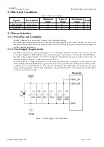
Page 15: ...y Requirements The NM1 module s power design is important to its performance The NM1 module can be powered by the low dropout regulator LDO with low static current and output current up to 0 5 A or th...

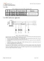
Page 16: ...lowing rules 1 Place the external SIM card holder near the NM1 module The external SIM card signal cable is 200 mm or shorter and is away from the RF cable and VBAT power cable 2 The SIM_VDD decouplin...

Page 17: ...dule is 1 8 V If the host level is 3 3 V add a level converter between the NM1 module and host The level converter that supports the SPI data rate is recommended Figure 3 4 shows the reference circuit...

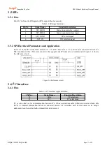
Page 18: ...tion Description 17 RXD Data receiving over the primary serial interface 18 TXD Data transmission over the primary serial interface 28 UART1_RXD Data receiving over the auxiliary serial interface 29 U...

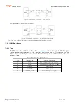
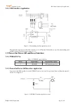
Page 19: ...e NM1 module has a USB 1 1 interface which can only be used for module upgrade If ESD design is required the maximum capacitance of ESD components must be less than 0 5 pF Otherwise waveform distortio...

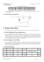
Page 20: ...wnloading add an LDO circuit to keep the circuit voltage at 3 3 V 3 9 Power On Power Off and Reset Interface 3 9 1 PWRKEY Pin Table 3 9 PWRKEY signal definition Pin No Signal Name Function Description...

Page 21: ...of the USB 1 1 signal cable is within 90 ohms Design general signal interfaces as required to match the interface signal level and prevent the NM1 module being damaged due to inconsistent levels The N...

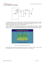
Page 22: ...he RF antenna peripheral circuit must have 50 ohms impedance In the recommended RF antenna peripheral circuit layout solution the RF cable is routed at layer 1 and the reference cable at layer 2 Use t...

Page 23: ...ipheral power circuit design place the decoupling capacitor near the power pin on the NM1 module keep high frequency and high speed circuits and sensitive circuits away from the PCB edges and isolate...

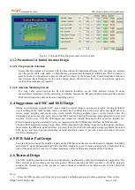
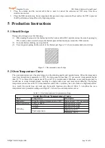
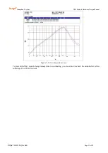
Page 24: ...ven temperature curve has great impact on the soldering quality and material status When the temperature rises from the ambient temperature to 150 C the rising speed is less than 3 C per second A temp...

Page 25: ...rdware Design Manual https www tuya com Page 25 of 29 Figure 5 2 Over temperature curve To prevent the NM1 module being damaged due to overheating you are advised to attach the module after reflow sol...

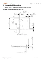
Page 26: ...gn Manual https www tuya com Page 26 of 29 6 Mechanical Dimensions This chapter describes the mechanical dimensions of the NM1 module in millimeters 6 1 NM1 Module Mechanical Dimensions Figure 6 1 Top...

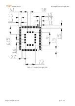
Page 27: ...Hangzhou Tuya Inc NM1 Module Hardware Design Manual https www tuya com Page 27 of 29 Figure 6 3 Transparent view unit mm...

Page 28: ...FCC Rules Operation is subject to the following two conditions 1 This device may not cause harmful interference 2 This device must accept any interference received including interference that may cau...

Page 29: ...encouraged to try to correct the interference by one or more of the following measures Reorient or relocate the receiving antenna Increase the separation between the equipment and receiver Connect th...

Reviews: