


Hangzhou Tuya Inc.
NM1 Module Hardware Design Manual
https://www.tuya.com
Page 12 of 29
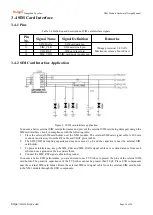
Pin No. Analog Signal
Definition
Pin Attribute
Input/
Output
Pin Voltage (V)
Remarks
3
SPI_MISO
Primary device input and
secondary device output
signal
I
1.8
N/A
4
SPI_MOSI
Primary device output
and secondary device
input signal
O
1.8
N/A
5
SPI_SCLK
Serial clock signal
O
1.8
N/A
6
SPI_CS
Chip selection signal
O
1.8
N/A
7
PWRKEY
Lower PWRKEY to
power on the NM1
module.
I
Maximum value of V
IL
: 0.3 x
VBAT
Minimum value of V
IH
: 0.7 x
VBAT
N/A
8
GPIO22
GPIO22
N/A
N/A
N/A
9
ADC0
Common analog-digit
conversion interface
I
0–1.4 V
N/A
10
SIM_GND
GND dedicated for the
SIM card
N/A
N/A
N/A
11
SIM_DATA
SIM card data signal
I/O
Maximum value of V
IL
: 0.25 x
SIM_VDD
Minimum value of V
IH
: 0.75 x
SIM_VDD
Maximum value of V
OL
: 0.15 x
SIM_VDD
Minimum value of V
OH
: 0.85 x
SIM_VDD
N/A
12
SIM_RST
SIM card reset signal
I/O
Maximum value of V
OL
: 0.15 x
SIM_VDD
Minimum value of V
OH
: 0.85 x
SIM_VDD
N/A
13
SIM_CLK
SIM card clock signal
I/O
Maximum value of V
OL
: 0.15 x
SIM_VDD
Minimum value of V
OH
: 0.85 x
SIM_VDD
N/A
14
SIM_VDD
SIM card power signal
O
1.8
N/A
15
RESET
Used to reset the NM1
module, which is active
at low level
I
N/A
N/A
16
NETLIGHT
Network status indication
O
N/A
N/A
17
RXD
Primary serial interface
that receives data
I
1.8
N/A
18
TXD
Primary serial interface
that transmits data
O
1.8
N/A
19
PSM_EINT
External interrupt
pin,
which is used to wake up
the NM1 module from
the PSM mode
I
N/A
N/A
20
SRCLKENAI
NFC interface
N/A
1.8
N/A


