User's Manual l MBa8MPxL UM 0100 l © 2022, TQ-Systems GmbH
Page 19
3.3.8
MIPI CSI
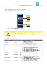
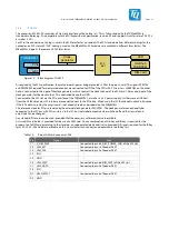
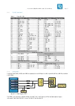
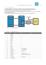
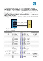
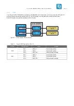
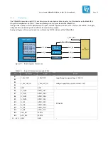
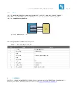
Both MIPI CSI interfaces provided by the TQMa8MPxL are routed to connector X57 on the bottom of the MBa8MPxL.
With a single camera, up to 4k at 45 FPS are supported, when using two cameras, the support splits to 1080p at 80 fps each.
Both CSI interfaces provide an I
2
C bus, four GPIO signals (reset, power enable, trigger, sync) and a master clock output on the
connector.
The GPIO signals of the CSI0 interface are connected to the ECSPI1 signals, which are multiplexed as GPIO for this purpose. The
GPIO signals of CSI1 are not connected by default due to missing software support. Instead, the ECSPI2 interface is provided on a
pin header. If a use as GPIO is required, this can be made possible by equipping 0 Ω resistors.
The I
2
C buses operate at 1.8 V and are connected to I2C4 via a level shifter on the MBa8MPxL. CSI0 can optionally be connected
to another I
2
C bus
to avoid address conflicts.
The master clock signals can be connected to the Clock Control Module of the i.MX 8M Plus. Via this Clock Control Module both
CSIs can be supplied with a reference clock each. The 0 Ω bridge for the connection is not assembled by default.
5 V are provided at pins 56, 58 and 60. This voltage may be loaded with a maximum of 300 mA.
TQMa8MPxL
MIPI_CSI0
MIPI_CSI1
TQ Camera
Adapter
5 V / 300 mA
2x CSI_I2C
ECSPI1
TRIGGER, SYNC,
PWR und RST
ECSPI2
TRIGGER, SYNC,
PWR und RST
CLK[2:1]_OUT
Figure 16: Block diagram MIPI CSI
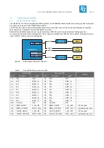
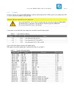
Table 13:
Pinout MIPI CSI, X57
Remark
Signal
Pin
Signal
Remark
–
GND
1
2
GND
–
10 kΩ PD
MIPI_CSI0_EN
3
4
MIPI_CSI1_EN
(NC), 10 kΩ PD
10 kΩ PD
MIPI_CSI0_RST#
5
6
MIPI_CSI1_RST#
(NC), 10 kΩ PD
–
MIPI_CSI0_TRIGGER
7
8
MIPI_CSI1_TRIGGER
(NC)
–
MIPI_CSI0_SYNC
9
10
MIPI_CSI1_SYNC
(NC)
–
(NC)
11
12
(NC)
–
–
GND
13
14
GND
–
–
MIPI_CSI0_DATA[3]_N
15
16
MIPI_CSI1_DATA[3]_N
–
–
MIPI_CSI0_DATA[3]_P
17
18
MIPI_CSI1_DATA[3]_P
–
–
GND
19
20
GND
–
–
MIPI_CSI0_DATA[2]_N
21
22
MIPI_CSI1_DATA[2]_N
–
–
MIPI_CSI0_DATA[2]_P
23
24
MIPI_CSI1_DATA[2]_P
–
–
GND
25
26
GND
–
–
MIPI_CSI0_DATA[1]_N
27
28
MIPI_CSI1_DATA[1]_N
–
–
MIPI_CSI0_DATA[1]_P
29
30
MIPI_CSI1_DATA[1]_P
–
–
GND
31
32
GND
–
–
MIPI_CSI0_DATA[0]_N
33
34
MIPI_CSI1_DATA[0]_N
–
–
MIPI_CSI0_DATA[0]_P
35
36
MIPI_CSI1_DATA[0]_P
–
–
GND
37
38
GND
–
–
MIPI_CSI0_CLK_N
39
40
MIPI_CSI1_CLK_N
–
–
MIPI_CSI0_CLK_P
41
42
MIPI_CSI1_CLK_P
–
–
GND
43
44
GND
–
Optional I2C_SDA_1V8
MIPI_CSI0_SDA
45
46
MIPI_CSI1_SDA
–
Optional I2C_SCL_1V8
MIPI_CSI0_SCL
47
48
MIPI_CSI1_SCL
–
–
GND
49
50
GND
–
0 Ω in series; (NP)
MIPI_CSI0_MCLK_OUT
51
52
MIPI_CSI1_MCLK_OUT
0 Ω in series; (NP);
routed to TP243
–
GND
53
54
GND
–
–
(NC)
55
56
V_5V_SW
Max. 300 mA
–
(NC)
57
58
–
(NC)
59
60


