
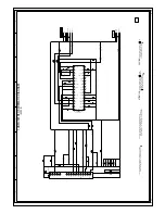


ABC
D
E
F
G
H
ABC
D
E
F
G
H
2
1
3
4
5
6
7
8
2
1
3
4
5
6
7
8
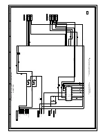
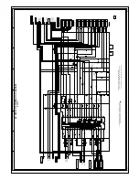
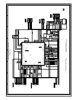
IC3201
BA00BC0WFP-E2
P.CON+3.3V_REG IC
12
45
6
IC3202
BD7820FP-E2
P.CON+1.8V_REG IC
12
45
6
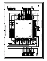
CP3201
CU2A1001
1
10
2
3
4
5
6
7
8
9
D3206
EC31QS04
D3207
EC31QS04
C3215
220
6.3V
YK
W825
C3210
220
6.3V
YK
C3202
470PCH
C3201
470PCH
C3213
1
F
C3208
1
F
C3205
470PCH
C3204
470PCH
C3209
1
F
C3214
1
F
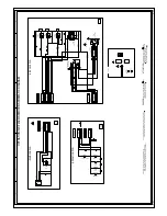
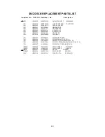
OF PRINTING AND SUBJECT TO CHANGE WITHOUT NOTICE
NOTE:
THIS SCHEMATIC DIAGRAM IS THE LATEST AT THE TIME
DANS LA NOMENCLATURE DES PIECES
N’UTILISER QUE CELLS DECRITES
DANGEREUSES AN POINT DE VUE SECURITE
:LES PIECES REPAREES PAR UN
ETANT
ATTENTION
:SINCE THESE PARTS MARKED BY
CAUTION
DESCRIBED IN PARTS LIST ONLY
CRITICAL FOR SAFETY,USE ONES
ARE
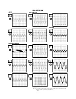
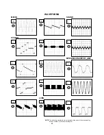
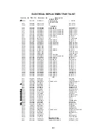
WAS RECEIVED IN GOOD CONDITION AND PICTURE IS NORMAL.
WITH THE DIGITAL TESTER WHEN THE COLOR BROADCAST
NOTE:THE DC VOLTAGE AT EACH PART WAS MEASURED
R3229
220
+-1%
R3217
560
R3211
3.3K
+-1%
R3212
5.6K
+-1%
R3208
10K
R3216
560
R3221
1K
+-1%
R3219
10K
R3222
1.2K
+-1%
B3202
BLM18PG181SN1D
B3203
BLM18PG181SN1D
B3204
BLM18PG181SN1D
B3205
BLM18PG181SN1D
B3206
BLM18PG181SN1D
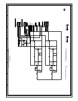
LCD+3.3V
P.CON+5V
P.CON+3.3V
AT+3.3V
P.CON+1.8V
GND
GND
SCALER-H
P.CON+3.3V
GND
AT+3.3V
AT+5V
AT+5V
P.CON+3.3V
LCD+3.3V
GND
SCALER-H
P.CON+3.3V
P.CON+1.8V
P.CON+5V
AT+5V
GND
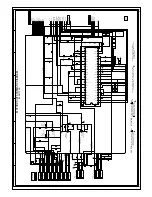
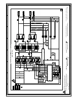
(CP3804)
TO SCALER
TO LVDS
TO SYNC SEPA
FROM/TO MICON
FROM POWER
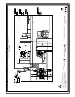
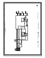
4.0
4.0
0
3.4
1.3
CTL
IN
GND
OUT
ADJ
AT+3.3V
GND
GND
GND
AT+5V
AT+3.8V
AT+3.8V
P.CON+9V
P.CON+5V
NC
LCD+3.3V
CTL
IN
GND
OUT
ADJ
3.5
3.8
0
1.9
0.75
(SCALER PCB)
REGULATOR SCHEMATIC DIAGRAM
H-34
H-33
PCBDS0
CEF174


