


ABC
D
E
F
G
H
ABC
D
E
F
G
H
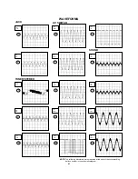
2
1
3
4
5
6
7
8
2
1
3
4
5
6
7
8
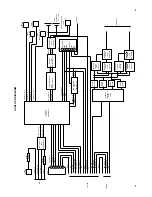
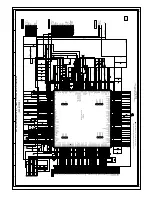
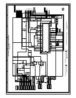
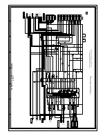
DURING PLAYBACK.
MEASURED WITH THE DIGITAL TESTER
NOTE:THE DC VOLTAGE EACH PART WAS
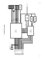
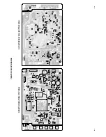
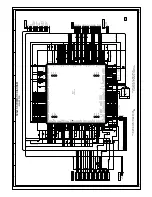
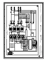
CP2251
A2001WR2-2P
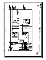
1
2
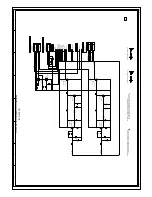
SW2251_2
EVQ21505R
EJECT_2
SW2252_2
EVQ21505R
STOP_2
SW2253_2
EVQ21505R
PLAY_2
SW2254_2
EVQ21505R
SKIP+_2
SW2255_2
EVQ21505R
SKIP-_2
OF PRINTING AND SUBJECT TO CHANGE WITHOUT NOTICE
NOTE:
THIS SCHEMATIC DIAGRAM IS THE LATEST AT THE TIME
R2255
6.8K
R2254
2.7K
R2252
1K
R2251
820
R2253
1.5K
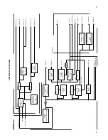
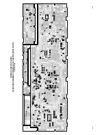
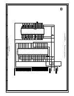
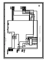
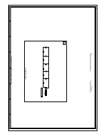
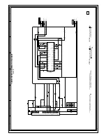
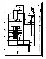
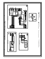
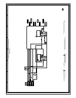
(OPERATION2 PCB)
OPERATION2 SCHEMATIC DIAGRAM
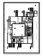
H-12
H-11
(CD2202)
PCB280
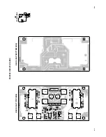
GND
KEY1
DEF092
FROM/TO OPERATION/REMOCON