EUROPA SERIES USER MANUAL
19
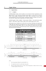
7-1-1 LVCMOS
LVCMOS digital video can be turned on or off with control commands. In the
open state, you can choose to output raw data (ORG) or non-uniform correction
(NUC) data, image processing (DRC) data. When choosing to use image
processing (DRC) data, the movement component does not support the function
of electronic variable and temperature information display.
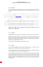
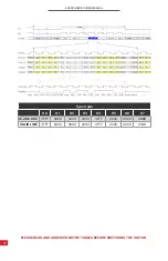
LVCMOS digital video includes 1 Clock signal (Clock), 1 line valid (Line_Valid)
signal, 1 valid frame signal (Frame_Valid), and 14 data signals (dv0-dv13).
Pixel data bits are divided into 10-bit and 14-bit. When RAW data or temperature
(TMP) data are produced, the data bits are 14-bits, namely DV[13:0], where DV0
is LSB and DV13 is the MSB. When the user selects the data after the output
image processing (DRC), the data bits are 10-bits, namely DV[9:0], where DV0 is
LSB and DV9 is for the MSB.
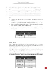
LVCMOS Clock Frequency
Model
Clock Frequency
Europa-C 380/
Europa-SL 380
12.857 MHz
Europa-C 640/
Europa-SL 640
19.286 MHz
Europa 380
6.4286 MHz
Europa 640
12.857 MHz
Note:
1.
Clock rising edge sampling is recommended for DV.
2�
The high level is valid for Line_Valid and Frame_Valid.
3.
After Line_Valid is valid it lasts for n Clock, which corresponds to the data of the first column
to the last column of the row in turn.
7-1 Digital Video
7.
Digital Video


