background image

www.ti.com

2.5.2

Read Operations

Address

translation

commands

Outbound

Outbound
command

FIFO

data

Return

FIFO

data

FIFO

Return

command

Inbound

FIFO

Registers

translation

Address

TxSM

8B/10B

encoding

Serializer

commands

Inbound

RxSM

Deserializer

decoding

8B/10B

Serial
TxData

Serial
RxData

System clock

Address

translation

Registers

commands

Inbound

translation

Address

commands

Outbound

8B/10B

decoding

FIFO

FIFO

command

Inbound

data

Return

FIFO

RxSM

Deserializer

RxData

Serial

encoding

8B/10B

VLYNQ Clock

command

Return

data

FIFO

Outbound

TxSM

Serializer

TxData

Serial

Slave

config bus

interface

VLYNQ Clock

System clock

Local VLYNC

Remote VLYNQ

Master

config bus

interface

Slave

config bus

interface

Master

config bus

interface

Peripheral Architecture

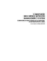
Read requests from the slave configuration bus interface are written to the outbound CMD FIFO (similar to
the write requests). Data is subsequently read from the FIFO and encapsulated into a read request
packet. The packet is encoded and serialized before it is transmitted to the remote device. Next, the
remote device deserializes, decodes the receive data, and writes the receive data to the inbound CMD
FIFO. After reading the address from the FIFO, a master configuration bus interface read operation
initiates in the remote device. When the remote master configuration bus interface receives the read data,
the data is written to the return data FIFO before it is encoded and serialized. When the receive data
reaches the local VLYNQ module, it is deserialized, decoded, and written to the return data FIFO (local
device). Finally, the read data is transferred on the local device’s slave configuration interface.

The data flow between two connected VLYNQ devices with read requests that originate from the DM644x
device is shown in

Figure 6

. The remote VLYNQ device returns the read data. Read data is shown with

dotted arrows.

Figure 6. Read Operations

SPRUE36A – September 2007

VLYNQ Port

15

Submit Documentation Feedback

Summary of Contents for VLYNQ Port

Page 1: ...TMS320DM644x DMSoC VLYNQ Port User s Guide Literature Number SPRUE36A September 2007...

Page 2: ...2 SPRUE36A September 2007 Submit Documentation Feedback...

Page 3: ...3 4 Interrupt Priority Vector Status Clear Register INTPRI 31 3 5 Interrupt Status Clear Register INTSTATCLR 31 3 6 Interrupt Pending Set Register INTPENDSET 32 3 7 Interrupt Pointer Register INTPTR...

Page 4: ...VLYNQ 2 0 Packet Format 41 A 4 VLYNQ 2 X Packets 43 Appendix B Write Read Performance 45 B 1 Write Performance 45 B 2 Read Performance 47 Appendix C Revision History 48 4 Contents SPRUE36A September 2...

Page 5: ...et Register INTPENDSET 32 15 Interrupt Pointer Register INTPTR 32 16 Transmit Address Map Register XAM 33 17 Receive Address Map Size 1 Register RAMS1 34 18 Receive Address Map Offset 1 Register RAMO1...

Page 6: ...ap Offset 1 Register RAMO1 Field Descriptions 34 17 Receive Address Map Size 2 Register RAMS2 Field Descriptions 35 18 Receive Address Map Offset 2 Register RAMO2 Field Descriptions 35 19 Receive Addr...

Page 7: ...rol of the device In general the ARM is responsible for configuration and control of the device including the DSP subsystem the video processing subsystem and a majority of the peripherals and externa...

Page 8: ...ital signal processor DSP enhanced direct memory access EDMA2 to the TMS320DM644x Digital Media System on Chip DMSoC EDMA3 This document summarizes the key differences between the EDMA3 and the EDMA2...

Page 9: ...M644x DMSoC serializes a write transaction to the remote external device and transfers the write via the VLYNQ port TX pins The remote VLYNQ module deserializes the transaction on the other side The r...

Page 10: ...e all multiplexed and sent across the same physical pins Supports both host peripheral and peer to peer communication models Simple block code packet formatting 8b 10b Supports in band and flow contro...

Page 11: ...egister CTRL The VLYNQ serial clock can be sourced from the internal system clock CLKDIR 1 or by an external clock source CLKDIR 0 for its serial operations The CLKDIV bit can divide the serial clock...

Page 12: ...er management Active low Low The request VLYNQ serial clock is active High The VLYNQ serial clock is requested to be high when all transactions are complete VLYNQ_RXD 0 3 VLYNQ receive data I VLYNQ re...

Page 13: ...NQ Module Structure The VLYNQ core module implements two 32 bit configuration bus interfaces Transmit operations and control register access require the slave configuration bus interface The master co...

Page 14: ...nfig bus interface Slave config bus interface Peripheral Architecture Write requests that initiate from the slave configuration bus interface of the local device write to the outbound command CMD FIFO...

Page 15: ...ata is subsequently read from the FIFO and encapsulated into a read request packet The packet is encoded and serialized before it is transmitted to the remote device Next the remote device deserialize...

Page 16: ...as a part of the initialization sequence For a connection between two VLYNQ devices of version 2 0 and later VLYNQ on DM644x device is version 2 6 the negotiation protocol using the available serial p...

Page 17: ...the local device sends the data with an address offset from the transmit address VLYNQ allows each receive packet address to be translated into one of the four mapped regions The size and offset of ea...

Page 18: ...lowing shows an example illustrating the address translation used in each VLYNQ module Address bits 31 26 are not used for address translation to remote devices on the DM644x device Table 3 illustrate...

Page 19: ...Q Module Remote VLYNQ Module TX Address Map Do not care 0400 0000h RX Address Map Size 1 0000 0100h Do not care RX Address Map Offset 1 0200 0000h Do not care RX Address Map Size 2 0000 0100h Do not c...

Page 20: ...s Map Size 1 Register RX Address Map Size 2 Register else if RX Packet Address RX Address Map Size 1 Register RX Address Map Size 2 Register RX Address Map Size 3 Register RX Address Map Size 4 Regist...

Page 21: ...etting one of the VLYNQ devices after two or more VLYNQ devices have established a link If only one of the VLYNQ devices is in reset then no data activity can occur across the serial interface during...

Page 22: ...SET when INTLOCAL 1 VLYNQ interprets bit 0 as the highest priority and it interprets bit 31 as the lowest priority The value that is returned when read is the vector of the highest priority interrupt...

Page 23: ...QINT to be asserted to the ARM CPU To ensure that serial bus errors result in interrupts to notify the application software you must perform the following steps 1 Set the INTENABLE bit to 1 in the VLY...

Page 24: ...s internally sourced you can use the CLKDIV bit in the VLYNQ control register CTRL to divide the serial clock down This saves normal mode operation power consumption at the expense of reduced performa...

Page 25: ...n the two devices Table 6 VLYNQ Port Controller Registers Offset Acronym Register Description Section 0h REVID Revision Register Section 3 1 4h CTRL Control Register Section 3 2 8h STAT Status Registe...

Page 26: ...re 9 Revision Register REVID 31 16 ID R 1h 15 8 7 0 REVMAJ REVMIN R 2h R 6h LEGEND R Read only n value after reset Table 7 Revision Register REVID Field Descriptions Bit Field Value Description 31 16...

Page 27: ...der to modify the value you must simultaneously write a 1 to the RTMVALIDWR bit 23 RTMVALIDWR RTM valid write bit 0 Will not allow writes to RXSAMPLEVAL bits 1 Will allow writes to RXSAMPLEVAL bits 22...

Page 28: ...int to a VLYNQ module local register typically the interrupt pending set register 6 3 Reserved 0 Reserved Always read as 0 Writes have no effect 2 AOPTDISABLE Address optimization disable 0 Address op...

Page 29: ...pins used 4h 4 RX pins used 5h Fh Reserved 23 20 SWIDTHOUT 0 Fh Size of the outbound serial data Indicates the number of transmit pins that are being used to establish the serial interface 0 No pins...

Page 30: ...d FIFO is not empty 5 NFEMPTY2 FIFO 2 is not empty 0 Indicates that the slave data FIFO is empty 1 Indicates that the slave data FIFO is not empty 4 NFEMPTY1 FIFO 1 is not empty 0 Indicates that the m...

Page 31: ...gister 30 5 Reserved 0 Reserved Always read as 0 Writes have no effect When read this field displays the vector that is mapped to the highest priority interrupt bit that is 4 0 INSTAT 0 1Fh pending fr...

Page 32: ...LOCAL 0 in CTRL interrupt packet is sent on the serial interface If INTLOCAL 1 in CTRL VLYNQ module interrupt VLQINT is asserted The interrupt pointer register INTPTR typically contains the address of...

Page 33: ...0 TXADRMAP Reserved R W 0 R 0 LEGEND R W Read Write R Read only n value after reset Table 14 Address Map Register XAM Field Descriptions Bit Field Value Description 31 2 TXADRMAP 0 3FFF FFFFh This fie...

Page 34: ...dress map offset 1 register RAMO1 to obtain the translated address 1 0 Reserved 0 Reserved Always read as 0 Writes have no effect The receive address map offset 1 register RAMO1 is used with the recei...

Page 35: ...ddress map offset 2 register RAMO2 to obtain the translated address 1 0 Reserved 0 Reserved Always read as 0 Writes have no effect The receive address map offset 2 register RAMO2 is used with the rece...

Page 36: ...dress map offset 3 register RAMO3 to obtain the translated address 1 0 Reserved 0 Reserved Always read as 0 Writes have no effect The receive address map offset 3 register RAMO3 is used with the recei...

Page 37: ...ddress map offset 4 register RAMO4 to obtain the translated address 1 0 Reserved 0 Reserved Always read as 0 Writes have no effect The receive address map offset 4 register RAMO4 is used with the rece...

Page 38: ...Read only n value after reset Table 23 Chip Version Register CHIPVER Field Descriptions Bit Field Value Description 31 16 DEVREV 0 FFFFh Device revision This field reflects the value of the device rev...

Page 39: ...Remote Revision Register 84h RCTRL Remote Control Register 88h RSTAT Remote Status Register 8Ch RINTPRI Remote Interrupt Priority Vector Status Clear Register 90h RINTSTATCLR Remote Interrupt Status C...

Page 40: ...6 DC 1101 1100 001111 0110 110000 1001 K28 7 FC 1111 1100 001111 1000 110000 0111 K23 7 F7 1111 0111 111010 1000 000101 0111 K27 7 FB 1111 1011 110110 1000 001001 0111 K29 7 FD 1111 1101 101110 1000...

Page 41: ...ow control disable request is transmitted by a VLYNQ module when RX FIFO resources are available to accommodate additional data The error indication is transmitted when errors are detected within a pa...

Page 42: ...ncluded only if ADRMASK 0 is set to 1 If ADRMASK 0 is cleared to 0 assume this byte is equal to bits 7 0 of the previous address Read response packets do not include this field ADDRESS 15 8 Address by...

Page 43: ...a channel L Link pulse and what is in italics is optional data up to 16 words total Packet with byte enables WriteBurst claaaaMMddMMddMMddT The above packet wrote to the LS half words from the specifi...

Page 44: ...et is now under way A flow is now received for channel 1 but it is soon disabled so the channel 1 packet continues The flow is enabled for channel one again quickly after flow is released for channel...

Page 45: ...direction interface the raw data is 99 4 or 396 Mbps After the 8B10B encoding is removed the maximum write rate is 396 0 8 316 8 Mbps The total throughput on the VLYNQ interface includes both transmi...

Page 46: ...Mbits sec Mbytes sec Mbits sec Mbytes sec 1 1 24 19 3 02 31 68 3 96 4 42 07 5 26 55 09 6 89 8 49 62 6 20 64 98 8 12 16 54 52 6 81 71 39 8 92 2 1 48 38 6 05 63 36 7 92 4 84 14 10 52 110 18 13 77 8 99 2...

Page 47: ...s combined Read Throughput data Read ReadReturn data max read rate Latency data max read rate Read ReadReturn data Latency max read rate For example with a 4 pin 99 MHZ VLYNQ connection for a single 3...

Page 48: ...ction 2 9 Changed fourth paragraph Added NOTE Table 8 Changed Description of INTLOCAL Section 3 17 Changed paragraph Figure 25 Changed DEVID reset value Table 23 Changed DEVID Description Figure A 1 C...

Page 49: ...ce and is an unfair and deceptive business practice TI is not responsible or liable for any such statements TI products are not authorized for use in safety critical applications such as life support...

Reviews: