background image


SPRS293A − OCTOBER  2005 − REVISED NOVEMBER 2005

57

POST OFFICE BOX 1443 

 HOUSTON, TEXAS 77251−1443

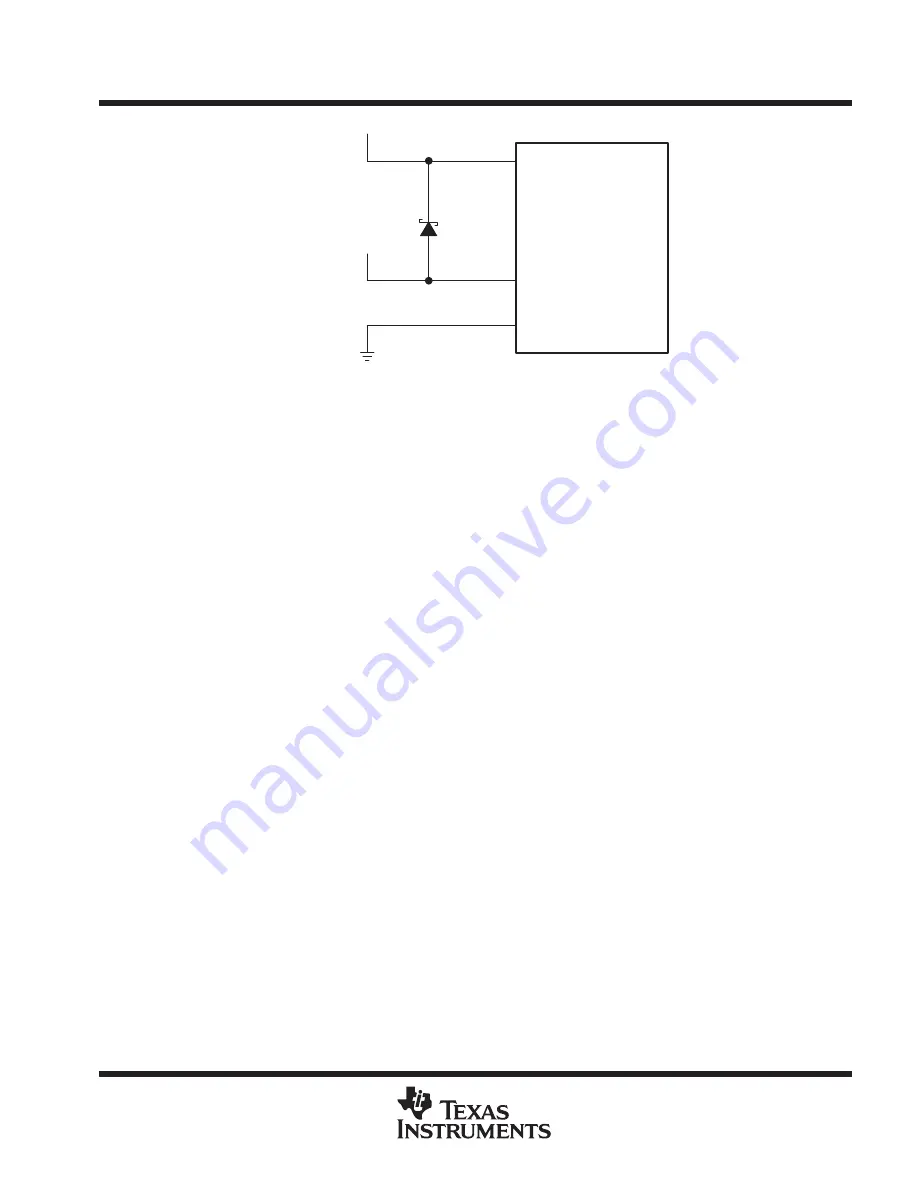
DVDD

CVDD

VSS

C6000

DSP

Schottky

Diode

I/O Supply

Core Supply

GND

Figure 13. Schottky Diode Diagram

Core and I/O supply voltage regulators should be located close to the DSP (or DSP array) to minimize
inductance and resistance in the power delivery path. Additionally, when designing for high-performance
applications utilizing the C6000

 platform of DSPs, the PC board should include separate power planes for

core, I/O, and ground, all bypassed with high-quality low-ESL/ESR capacitors.

power-supply decoupling 

In order to properly decouple the supply planes from system noise, place as many capacitors (caps) as possible
close to the DSP. Assuming 0603 caps, the user should be able to fit a total of 60 caps — 30 for the core supply
and 30 for the I/O supply. These caps need to be close (no more than 1.25 cm maximum distance) to the DSP
to be effective. Physically smaller caps are better, such as 0402, but the size needs to be evaluated from a
yield/manufacturing point-of-view. Parasitic inductance limits the effectiveness of the decoupling capacitors,
therefore physically smaller capacitors should be used while maintaining the largest available capacitance
value. As with the selection of any component, verification of capacitor availability over the product’s production
lifetime needs to be considered.

Summary of Contents for TMS320C6712D

Page 1: ...r 16 Independent Channels D 16 Bit External Memory Interface EMIF Glueless Interface to Asynchronous Memories SRAM and EPROM Glueless Interface to Synchronous Memories SDRAM and SBSRAM 256M Byte Total...
Page 2: ...multichannel buffered serial port timing 86 timer timing 95 general purpose input output GPIO port timing 96 JTAG test port timing 97 mechanical data 98 revision history 3 GDP and ZDP BGA package bot...

Page 3: ...e Big Endian Format section Added Note 26 Terminal Functions Resets and Interrupts section Updated IPU IPD for RESET Signal Name from IPU to 29 Terminal Functions Reserved for Test section Changed IPU...

Page 4: ...OUSTON TEXAS 77251 1443 PAGE S NO ADDITIONS CHANGES DELETIONS 83 RESET TIMING section Added Note 88 MULTICHANNEL BUFFERED SERIAL PORT TIMING switching characteristics over recommended operating condit...

Page 5: ...2005 5 POST OFFICE BOX 1443 HOUSTON TEXAS 77251 1443 GDP and ZDP BGA package bottom view GDP and ZDP 272 PIN BALL GRID ARRAY BGA PACKAGE BOTTOM VIEW 2 4 6 8 20 18 16 14 12 10 M E A 1 C B D G F H K J L...

Page 6: ...s a two level cache based architecture and has a powerful and diverse set of peripherals The Level 1 program cache L1P is a 32 Kbit direct mapped cache and the Level 1 data cache L1D is a 32 Kbit 2 wa...

Page 7: ...cy 32 Bit Timers 1 2 of SYSCLK2 2 GPIO Module SYSCLK2 1 Size Bytes 72K On Chip Memory Organization 4K Byte 4KB L1 Program L1P Cache 4KB L1 Data L1D Cache 64KB Unified Mapped RAM Cache L2 CPU ID CPU Re...

Page 8: ...t 167 MHz The C6712 device runs at 100 MHz clock speed and the C6712C C6712D device runs at 150 MHz clock speed D The C6211 C6211B C6711 100 C6711B and C6712 devices have a core voltage of 1 8 V the C...

Page 9: ...sters Control Logic In Circuit Emulation Interrupt Control Framing Chips H 100 MVIP SCSA T1 E1 AC97 Devices SPI Devices Codecs Digital Signal Processor In addition to fixed point instructions these fu...

Page 10: ...cle Another key feature of the C67x CPU is the load store architecture where all instructions operate on registers as opposed to data in memory Two sets of data addressing units D1 and D2 are responsi...

Page 11: ...dst src2 src2 src2 src2 src2 src2 src2 long src long src long dst long dst long src 8 8 8 2X 1X L2 S2 M2 D2 D1 M1 S1 L1 Control Register File DA1 DA2 ST1 LD1 32 LSB LD2 32 LSB LD2 32 MSB 32 32 Data Pa...

Page 12: ...0197 FFFF Timer 1 Registers 256K 0198 0000 019B FFFF Interrupt Selector Registers 512 019C 0000 019C 01FF Device Configuration Registers 4 019C 0200 019C 0203 Reserved 256K 516 019C 0204 019F FFFF EDM...

Page 13: ...WIBAR L2 writeback invalidate base address register 0184 4014 L2WIWC L2 writeback invalidate word count register 0184 4020 L1PIBAR L1P invalidate base address register 0184 4024 L1PIWC L1P invalidate...

Page 14: ...ther Event 01A0 0030 01A0 0047 Parameters for Event 2 6 words or Reload Link Parameters for other Event 01A0 0048 01A0 005F Parameters for Event 3 6 words or Reload Link Parameters for other Event 01A...

Page 15: ...DMA event selector 3 01A0 FF1F 01A0 FFDC Reserved 01A0 FFE0 PQSR Priority queue status register 01A0 FFE4 CIPR Channel interrupt pending register 01A0 FFE8 CIER Channel interrupt enable register 01A0...

Page 16: ...7 C118 PLLDIV1 PLL controller divider 1 register 01B7 C11C PLLDIV2 PLL controller divider 2 register 01B7 C120 PLLDIV3 PLL controller divider 3 register 01B7 C124 OSCDIV1 Oscillator divider 1 register...

Page 17: ...RIPTION McBSP0 McBSP1 ACRONYM REGISTER DESCRIPTION 018C 0000 0190 0000 DRRx McBSPx data receive register via Configuration Bus The CPU and EDMA controller can only read this register they cannot write...

Page 18: ...ARE SDCAS SSADS BIG LITTLE ENDIAN BOOTMODE EMIFBE BOOTMODE1 BOOTMODE0 The CLKOUT2 pin is multiplexed with the GP 2 pin Default function is CLKOUT2 To use this pin as GPIO the GP2EN bit in the GPEN reg...

Page 19: ...X0 CLKR0 FSR0 DR0 CLKS0 Timer 1 Receive Receive Timer 0 Timers McBSP1 McBSP0 Transmit Transmit Clock Clock McBSPs Multichannel Buffered Serial Ports TINP1 TINP0 For proper device operation these pins...

Page 20: ...eset device configurations at device reset Table 14 describes the device configuration pins which are set up via internal or external pullup pulldown resistors through the LENDIAN EMIFBE BOOTMODE 1 0...

Page 21: ...an Mode Correctness portion of this data sheet LENDIAN B17 Device Endian mode LEND 0 System operates in Big Endian mode The EMIFBE pin must be pulled low 1 System operates in Little Endian mode defaul...

Page 22: ...16 Reserved RW 0 15 5 4 3 0 Reserved EKSRC Reserved RW 0 R W 0 R W 0 Legend R W Read Write n value after reset Do not write non zero values to these bit locations Table 16 Device Configuration DEVCFG...

Page 23: ...dentifies the external signal names the associated pin ball numbers along with the mechanical package designator the pin type I O Z or I O Z whether the pin has any internal pullup pulldown resistors...

Page 24: ...PLLHV C5 A Analog power 3 3 V for PLL JTAG EMULATION TMS B7 I IPU JTAG test port mode select TDO A8 O Z IPU JTAG test port data out TDI A7 I IPU JTAG test port data in TCK A6 I IPU JTAG test port cloc...

Page 25: ...an external pullup pulldown resistor BOOTMODE1 BOOTMODE0 C19 C20 I IPD Bootmode 1 0 00 Emulation boot 01 CE1 width 8 bit asynchronous external ROM boot with default timings default mode 10 CE1 width...

Page 26: ...word address CE1 W18 O Z IPU Enabled by bits 28 through 31 of the word address Only one asserted during any external data access CE0 V17 O Z IPU Only one asserted during any external data access BE1...

Page 27: ...i EA12 V14 O Z IPU Note EMIF address numbering for the device start with EA2 to maintain signal name compati bility with other C671x devices e g C6711 C6713 see the 16 bit EMIF addressing scheme in EA...

Page 28: ...Because it is common for some ICs to 3 state their out puts at times a 10 k pullup resistor may be desirable even when an external device is driving the pin CLKR1 M1 I O Z IPD Receive clock CLKX1 L3 I...

Page 29: ...I O Z GP 7 EXT_INT7 E3 External interrupts Edge driven Polarity independently selected via the External Interrupt Polarity Register GP 6 EXT_INT6 D2 I O Z IPU Edge driven Polarity independently selec...

Page 30: ...power or ground RSV D7 IPD Reserved leave unconnected do not connect to power or ground RSV A12 Reserved For new designs it is recommended that this pinbe connected directly to CVDD core power For ol...

Page 31: ...DESCRIPTION SIGNAL NAME GDP ZDP TYPE IPD IPU DESCRIPTION ADDITIONAL RESERVED FOR TEST R2 R3 T1 T2 U1 U2 RSV U3 Reserved leave unconnected do not connect to power or ground RSV V1 Reserved leave unconn...

Page 32: ...ly decoupling portion of this data sheet DVDD T3 S see the power supply decoupling portion of this data sheet U5 U7 U12 U16 V13 V15 V19 W3 W9 W12 Y7 Y17 A4 A9 A10 B2 CVDD B19 S 1 20 V supply voltage S...

Page 33: ...V supply voltage See Note see the power supply decoupling portion of this data sheet CVDD R4 S see the power supply decoupling portion of this data sheet R17 U6 U10 U11 U14 U15 V3 V18 W2 Note This val...

Page 34: ...ls J9 J12 K9 K12 L9 L12 M9 M12 shaded are all tied to ground and act as VSS L9 GND The center thermal balls J9 J12 K9 K12 L9 L12 M9 M12 shaded are all tied to ground and act as both electrical grounds...

Page 35: ...1443 Terminal Functions Continued SIGNAL PIN NO SIGNAL NAME GDP and ZDP TYPE DESCRIPTION GROUND PINS CONTINUED U13 U17 U20 W1 W5 W11 VSS W16 GND Ground pins VSS W20 GND Ground pins Y1 Y2 Y13 Y19 Y20...

Page 36: ...ing Editor C C Assembly Code Generation and Debug plus additional development tools Scalable Real Time Foundation Software DSP BIOS which provides the basic run time target software needed to support...

Page 37: ...ication testing TMDS Fully qualified development support product TMX and TMP devices and TMDX development support tools are shipped with the following disclaimer Developmental product is intended for...

Page 38: ...High Rel non 38535 GDP 272 pin plastic BGA ZDP 272 pin plastic BGA with Pb free soldered balls BGA Ball Grid Array QFP Quad Flatpack The ZDP mechanical package designator represents the version of the...

Page 39: ...devices associated development tools and third party support TMS320C6000 DSP Software Programmable Phase Locked Loop PLL Controller Reference Guide literature number SPRU233 describes the functionalit...

Page 40: ...e bit fields in the CPU CSR register For more detailed information on the bit fields in the CPU CSR register see the TMS320C6000 DSP Peripherals Overview Reference Guide literature number SPRU190 and...

Page 41: ...he a functional unit has priority over a clear by the MVC instruction if they occur on the same cycle The saturate bit is set one full cycle one delay slot after a saturate occurs This bit will not be...

Page 42: ...function and for silicon advisories concerning EDMA L2 memory accesses blocked see the TMS320C6712 TMS320C6712C TMS320C6712D Digital Signal Processors Silicon Errata literature number SPRZ182C or lat...

Page 43: ...00100 GPINT4 00100 GPINT4 GPIO INT_05 MUXL 9 5 00101 GPINT5 00101 GPINT5 GPIO INT_06 MUXL 14 10 00110 GPINT6 00110 GPINT6 GPIO INT_07 MUXL 20 16 00111 GPINT7 00111 GPINT7 GPIO INT_08 MUXL 25 21 01000...

Page 44: ...annel See Table 21 and Table 22 for the EDMA Event Selector registers and their associated bit descriptions Table 21 EDMA Channels Table 22 EDMA Selector EDMA CHANNEL EDMA SELECTOR CONTROL REGISTER DE...

Page 45: ...1A0 FF0C 31 30 29 28 27 24 23 22 21 20 19 16 Reserved EVTSEL15 Reserved EVTSEL14 R 0 R W 00 1111b R 0 R W 00 1110b 15 14 13 12 11 8 7 6 5 4 3 0 Reserved EVTSEL13 Reserved EVTSEL12 R 0 R W 00 1101b R 0...

Page 46: ...and PLLDIV2 registers SYSCLK3 CLKMODE0 EMIF Clock Input C6712D DSP PLLOUT PLLREF DIVIDER D0 OSCDIV1 DIVIDER D1 DIVIDER D2 DIVIDER D3 ECLKOUT 1 0 1 0 1 0 PLLHV C2 C1 EMI filter 3 3 V 10 F 0 1 F D0EN P...

Page 47: ...1EN 1 OSCDIV1 15 Derived from CLKIN ECLKOUT ON ENABLED derived from SYSCLK3 EKSRC 0 DEVCFG 4 EKEN 1 EMIF GBLCTL 5 SYSCLK3 selected default To select ECLKIN as source EKSRC 1 DEVCFG 4 and EKEN 1 EMIF G...

Page 48: ...Software Programmable Phase Locked Loop PLL Controller Reference Guide literature number SPRU233 SYSCLK2 is the internal clock source for peripheral bus control SYSCLK2 Divider D2 must be programmed...

Page 49: ...le This bit indicates if the clock input has stabilized 0 Clock input not yet stable Clock counter is not finished counting default 1 Clock input stable 5 4 Reserved Reserved Read only writes have no...

Page 50: ...SCRIPTION 31 5 Reserved Reserved Read only writes have no effect 4 0 PLLM PLL multiply mode default is x7 0 0111 00000 Reserved 10000 x16 00001 Reserved 10001 x17 00010 Reserved 10010 x18 00011 Reserv...

Page 51: ...BIT NAME DESCRIPTION 31 16 Reserved Reserved Read only writes have no effect 15 DxEN Divider Dx Enable where x denotes 0 through 3 0 Divider x Disabled No clock output 1 Divider x Enabled default The...

Page 52: ...L path Table 31 Oscillator Divider 1 Register OSCDIV1 BIT NAME DESCRIPTION 31 16 Reserved Reserved Read only writes have no effect 15 OD1EN Oscillator Divider 1 Enable 0 Oscillator Divider 1 Disabled...

Page 53: ...EN GP6 EN GP5 EN GP4 EN GP2 EN R W 0 R W 1 R W 1 R W 1 R W 1 R W 0 R W 0 R W 0 R W 0 Legend R W Readable Writeable n value after reset x undefined value after reset Figure 9 GPIO Enable Register GPEN...

Page 54: ...er down mode logic TMS320C6712D CLKOUT2 Figure 11 Power Down Mode Logic triggering wake up and effects The power down modes and their wake up methods are programmed by setting the PWRD field bits 15 1...

Page 55: ...bits in the CSR before the PD mode takes effect As best practice NOPs should be padded after the PWRD bits are set in the CSR to account for this delay If PD1 mode is terminated by a non enabled inte...

Page 56: ...ock source output signals may transition in response to stimulus on the inputs Under these conditions peripherals will not operate according to specifications The device includes a programmable PLL wh...

Page 57: ...ing In order to properly decouple the supply planes from system noise place as many capacitors caps as possible close to the DSP Assuming 0603 caps the user should be able to fit a total of 60 caps 30...

Page 58: ...PD on the TRST pin to ensure that TRST will always be asserted upon power up and the DSP s internal emulation logic will always be properly initialized when this pin is not routed out JTAG controllers...

Page 59: ...grades cannot meet EMIF input hold time Trace impedance 50 200 MHz 32 bit SDRAM 5 meet EMIF input hold time requirement see NOTE 1 125 MHz 16 bit SDRAM 8E 100 MHz 2 Loads One bank of two 1 2 to 3 inc...

Page 60: ...necessary to load valid code into internal memory The emulation driver will release the CPU from the stalled state at which point the CPU will vector to address 0 Prior to beginning execution the emul...

Page 61: ...VIH High level input voltage All signals except CLKS1 DR1 and RESET 2 V VIH High level input voltage CLKS1 DR1 and RESET 2 V VIL Low level input voltage All signals except CLKS1 DR1 and RESET 0 8 V VI...

Page 62: ...commended operating conditions table For more details on CPU peripheral and I O activity see the TMS320C62x C67x Power Consumption Summary application report literature number SPRA486 For the device t...

Page 63: ...is not necessary to add or subtract the transmission line delay 2 ns or longer from the data sheet timings 42 3 5 nH Device Pin see note Input requirements in this data sheet are tested with an input...

Page 64: ...nt specifications for Rise and Fall Time For device specific information on these values refer to the Recommended Operating Conditions section of this Data Sheet VOS max VIH min Minimum Risetime Wavef...

Page 65: ...els to attain accurate timing analysis for a given system see the Using IBIS Models for Timing Analysis application report literature number SPRA839 If needed external logic hardware such as buffers m...

Page 66: ...equirement 6 Control signal route delay 7 External device hold time 8 External device access time 9 DSP hold time requirement 10 DSP setup time requirement 11 Data route delay 1 2 3 4 5 6 7 8 10 11 EC...

Page 67: ...N frequency is 25 MHz use C 40 ns See the PLL and PLL Controller section of this data sheet CLKIN 1 2 3 4 4 Figure 21 CLKIN Timings switching characteristics over recommended operating conditions for...

Page 68: ...ns The reference points for the rise and fall transitions are measured at VOL MAX and VOH MIN C3 CLKOUT3 period in ns CLKOUT3 period is a divide down of the CPU clock configurable via the OSCDIV1 reg...

Page 69: ...H Pulse duration ECLKOUT high EH 0 9 EH 0 9 ns 3 tw EKOL Pulse duration ECLKOUT low EL 0 9 EL 0 9 ns 4 tt EKO Transition time ECLKOUT 2 ns 5 td EKIH EKOH Delay time ECLKIN high to ECLKOUT high 1 6 5 n...

Page 70: ...WS Write setup WST Write strobe WH Write hold These parameters are programmed via the EMIF CE space control registers switching characteristics over recommended operating conditions for asynchronous m...

Page 71: ...Ready Hold 2 BE Address Read Data 2 1 2 1 2 1 2 1 5 4 3 ARDY 7 7 6 6 5 ECLKOUT CE 3 0 EA 21 2 ED 15 0 AOE SDRAS SSOE ARE SDCAS SSADS BE 1 0 AWE SDWE SSWE AOE SDRAS SSOE ARE SDCAS SSADS and AWE SDWE SS...

Page 72: ...Ready Hold 2 BE Address Write Data 10 10 9 11 9 8 9 8 9 8 7 7 6 6 ECLKOUT CEx EA 21 2 ED 31 0 BE 3 0 ARDY AOE SDRAS SSOE ARE SDCAS SSADS AWE SDWE SSWE AOE SDRAS SSOE ARE SDCAS SSADS and AWE SDWE SSWE...

Page 73: ...OH CEV Delay time ECLKOUT high to CEx valid 1 2 7 ns 2 td EKOH BEV Delay time ECLKOUT high to BEx valid 7 ns 3 td EKOH BEIV Delay time ECLKOUT high to BEx invalid 1 2 ns 4 td EKOH EAV Delay time ECLKO...

Page 74: ...4 5 8 8 9 6 7 3 1 2 ARE SDCAS SSADS AOE SDRAS SSOE and AWE SDWE SSWE operate as SSADS SSOE and SSWE respectively during SBSRAM accesses Figure 28 SBSRAM Read Timing ECLKOUT CE 3 0 BE 1 0 EA 21 2 ED 1...

Page 75: ...time ECLKOUT high to CEx valid 1 5 7 ns 2 td EKOH BEV Delay time ECLKOUT high to BEx valid 7 ns 3 td EKOH BEIV Delay time ECLKOUT high to BEx invalid 1 5 ns 4 td EKOH EAV Delay time ECLKOUT high to E...

Page 76: ...ECLKOUT CE 3 0 BE 1 0 EA 11 2 ED 15 0 EA12 AOE SDRAS SSOE ARE SDCAS SSADS AWE SDWE SSWE EA 21 13 BE1 BE2 BE3 BE4 Bank Column D1 D2 D3 D4 8 7 6 5 5 5 1 3 2 8 4 4 4 1 READ ARE SDCAS SSADS AWE SDWE SSWE...

Page 77: ...ECLKOUT CE 3 0 BE 1 0 EA 11 2 ED 15 0 AOE SDRAS SSOE ARE SDCAS SSADS AWE SDWE SSWE EA12 EA 21 13 BE1 BE2 BE3 BE4 Bank Column D1 D2 D3 D4 11 8 9 5 5 5 4 2 11 8 9 4 4 2 1 10 3 4 WRITE ARE SDCAS SSADS AW...

Page 78: ...dress 12 5 5 5 1 EA 11 2 ACTV 12 4 4 4 1 ARE SDCAS SSADS AWE SDWE SSWE and AOE SDRAS SSOE operate as SDCAS SDWE and SDRAS respectively during SDRAM accesses Figure 32 SDRAM ACTV Command ECLKOUT CE 3 0...

Page 79: ...k 11 12 5 5 1 DEAC 11 12 4 4 1 ARE SDCAS SSADS AWE SDWE SSWE and AOE SDRAS SSOE operate as SDCAS SDWE and SDRAS respectively during SDRAM accesses Figure 34 SDRAM DEAC Command ECLKOUT CE 3 0 BE 1 0 EA...

Page 80: ...NCHRONOUS DRAM TIMING CONTINUED ECLKOUT CE 3 0 BE 1 0 EA 21 2 ED 15 0 AOE SDRAS SSOE ARE SDCAS SSADS AWE SDWE SSWE MRS value 11 8 12 5 1 MRS 11 8 12 4 1 ARE SDCAS SSADS AWE SDWE SSWE and AOE SDRAS SSO...

Page 81: ...mpedance to HOLDA low 0 2E ns 4 td HOLDH EMLZ Delay time HOLD high to EMIF Bus low impedance 2E 7E ns 5 td EMLZ HOLDAH Delay time EMIF Bus low impedance to HOLDA high 0 2E ns E ECLKIN period in ns EMI...

Page 82: ...77251 1443 BUSREQ TIMING switching characteristics over recommended operating conditions for the BUSREQ cycles see Figure 38 NO PARAMETER 150 UNIT NO PARAMETER MIN MAX UNIT 1 td EKOH BUSRV Delay time...

Page 83: ...TER MIN MAX UNIT 2 td RSTH ZV Delay time external RESET high to internal reset high and all signal groups valid CLKMODE0 1 512 x CLKIN period ns 3 td RSTL ECKOL Delay time RESET low to ECLKOUT high im...

Page 84: ...et Phase 1 The RESET pin is asserted During this time all internal clocks are running at the CLKIN frequency divide by 8 The CPU is also running at the CLKIN frequency divide by 8 Reset Phase 2 The RE...

Page 85: ...UNIT NO MIN MAX UNIT 1 tw ILOW Width of the NMI interrupt pulse low 2P ns 1 tw ILOW Width of the EXT_INT interrupt pulse low 4P ns 2 tw IHIGH Width of the NMI interrupt pulse high 2P ns 2 tw IHIGH Wid...

Page 86: ...signals is inverted then the timing references of that signal are also inverted P 1 CPU clock frequency in ns For example when running parts at 150 MHz use P 6 7 ns The minimum CLKR X period is twice...

Page 87: ...ce the CPU cycle time 2P and not faster than 75 Mbps 13 3 ns This means that the maximum bit rate for communications between the McBSP and other device is 75 Mbps for 150 MHz CPU clock where the McBSP...

Page 88: ...ON TEXAS 77251 1443 MULTICHANNEL BUFFERED SERIAL PORT TIMING CONTINUED Bit n 1 n 2 n 3 Bit 0 Bit n 1 n 2 n 3 14 13 12 11 10 9 3 3 2 8 7 6 5 4 4 3 1 3 2 CLKS CLKR FSR int FSR ext DR CLKX FSX int FSX ex...

Page 89: ...FSR external CLKR X no need to resync CLKR X needs resync Figure 42 FSR Timing When GSYNC 1 timing requirements for McBSP as SPI master or slave CLKSTP 10b CLKXP 0 see Figure 43 150 NO MASTER SLAVE UN...

Page 90: ...P_clks if CLKSM 0 P_clks CLKS period T CLKX period 1 CLKGDV S H CLKX high pulse width CLKGDV 2 1 S if CLKGDV is even CLKGDV 1 2 S if CLKGDV is odd or zero L CLKX low pulse width CLKGDV 2 S if CLKGDV...

Page 91: ...s CLKG is programmed as 1 2 of the CPU clock by setting CLKSM CLKGDV 1 S Sample rate generator input clock 2P if CLKSM 1 P 1 CPU clock frequency Sample rate generator input clock P_clks if CLKSM 0 P_c...

Page 92: ...DX high impedance following last data bit from CLKX high H 2 H 3 ns 7 tdis FXH DXHZ Disable time DX high impedance following last data bit from FSX high 2P 3 6P 17 ns 8 td FXL DXV Delay time FSX low t...

Page 93: ...LKX low T 2 T 3 ns 3 td CKXH DXV Delay time CLKX high to DX valid 3 4 6P 2 10P 17 ns 6 tdis CKXH DXHZ Disable time DX high impedance following last data bit from CLKX high 2 4 6P 3 10P 17 ns 7 td FXL...

Page 94: ...OCTOBER 2005 94 POST OFFICE BOX 1443 HOUSTON TEXAS 77251 1443 Bit 0 Bit n 1 n 2 n 3 n 4 Bit 0 Bit n 1 n 2 n 3 n 4 5 4 3 7 6 2 1 CLKX FSX DX DR Figure 46 McBSP Timing as SPI Master or Slave CLKSTP 11b...

Page 95: ...s P 1 CPU clock frequency in ns For example when running parts at 150 MHz use P 10 ns switching characteristics over recommended operating conditions for timer outputs see Figure 47 NO PARAMETER 150 U...

Page 96: ...Ix changes through software polling of the GPIO register the GPIx duration must be extended to at least 24P to allow the DSP enough time to access the GPIO register through the CFGBUS switching charac...

Page 97: ...5 ns 3 tsu TDIV TCKH Setup time TDI TMS TRST valid before TCK high 10 ns 4 th TCKH TDIV Hold time TDI TMS TRST valid after TCK high 7 ns switching characteristics over recommended operating conditions...

Page 98: ...air 19 2 0 8 R JA Junction to free air 18 4 0 9 PsiJB Junction to board 16 0 0 m s meters per second thermal resistance characteristics S PBGA package for ZDP NO C W Air Flow m s Two Signals Two Plan...

Page 99: ...weight in homogeneous materials Where designed to be soldered at high temperatures TI Pb Free products are suitable for use in specified lead free processes Green RoHS no Sb Br TI defines Green to me...

Page 100: ...D G F H K J L W R N P U T V Y 3 5 7 9 11 17 15 13 19 0 635 0 635 26 80 SQ 23 80 24 20 SQ 27 20 24 13 TYP 0 57 0 65 0 60 0 90 Seating Plane 0 50 0 70 2 57 MAX 0 15 0 10 A1 Corner 1 27 1 27 4204396 A 04...

Page 101: ...W R N P U T V Y 3 5 7 9 11 17 15 13 19 0 635 0 635 26 80 SQ 23 80 24 20 SQ 27 20 24 13 TYP 0 57 0 65 0 60 0 90 Seating Plane 0 50 0 70 2 57 MAX 0 15 0 10 A1 Corner 1 27 1 27 4204398 A 04 02 Bottom Vi...

Page 102: ...ute a license from TI to use such products or services or a warranty or endorsement thereof Use of such information may require a license from a third party under the patents or other intellectual pro...

Reviews: