Vcc
GND
B
A
D
R
1
2
4
5
6
7
8
DE
3
U1
RE
DUT_VCC
R5
60
W
0V
5V
Receive
data
B
A
Transmit
data
V
OD
375
W
R8
375
W
R9
V
CM
= -7V to +12V
5V
PSU1
V
CM
PSU2
Scope
Ch4
Ch3
Ch2
Ch1
5V
Signal
Generator
JMP4
1
2
VCC
3
4
R
D
JMP3
1
2
VCC
3
4
JMP2
1
2
VCC
3
4
/RE
DE
JMP6
1
2
3
4
1
JMP11
2
3
1
JMP14
2
3
1
2
3
TB1
G
N
D
E
A
R
T
H
V
C
C
HVD96
EVM
JMP7
1
2
3
4
R9
375
W
R8
375
W
Powering up the EVM and Taking Measurements
www.ti.com
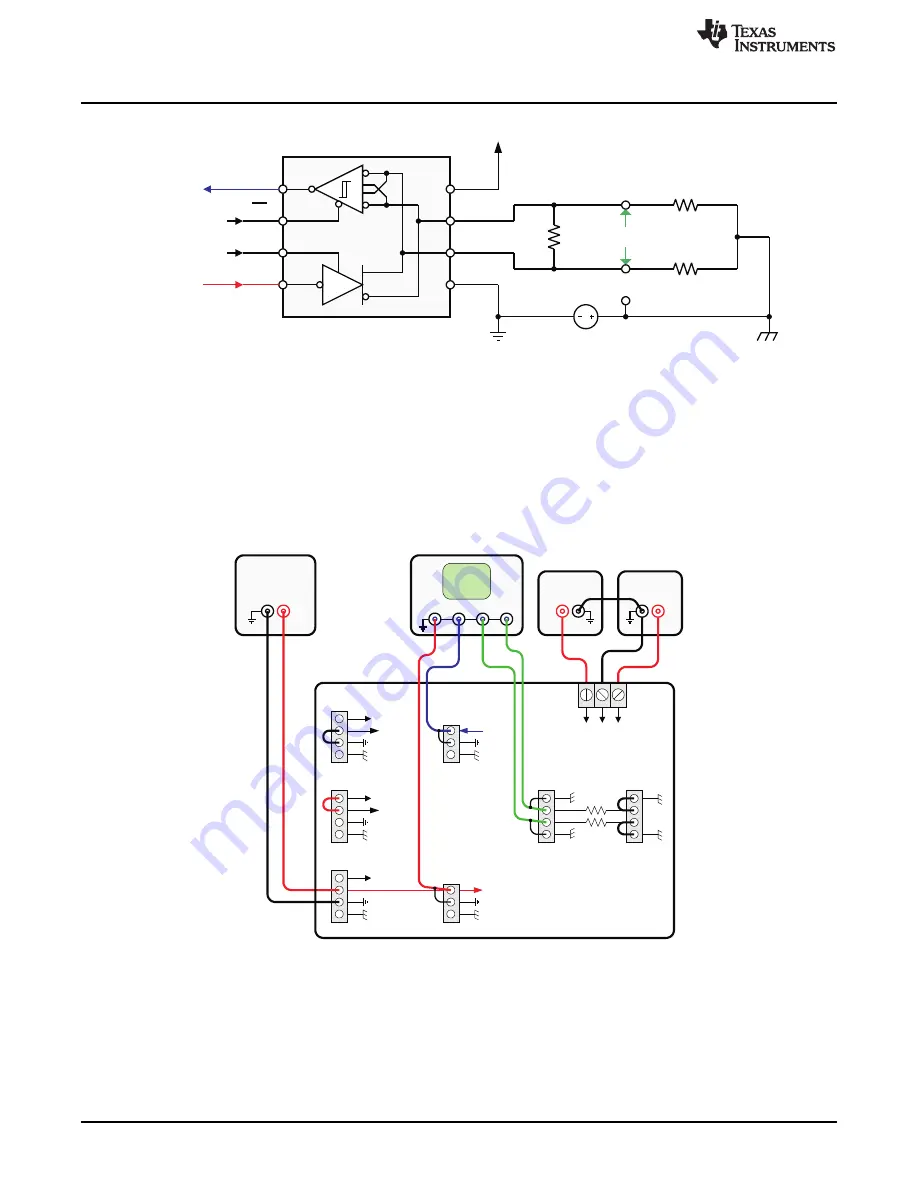
Figure 7. Configuration for Maximum Loading
While the cable connections of the signal generator and the oscilloscope remain the same as in the
previous example, the following board changes need to be implemented to reflect maximum load
conditions:
•
replace R5 (120
Ω
default) with 60
Ω
•
replace R8 and R9 (0
Ω
default) with 375
Ω
•
connect pin 2 of JMP7 with pin 1 and pin 3 with pin 4
•
replace the previous wire-bridge at TB1 with a second power supply unit (PSU2) and connect the
ground terminals of both, PSU1 and PSU2 with a wire-bridge, as shown in
Figure 8. EVM Set-up for Maximum Loading
Note that
only shows the wiring of PSU2 for positive common-mode voltages. For negative
V
CM
, connect the ground terminal of PSU2 with pin 1 of TB1 (Earth), and the V
CM
-output of PSU2 with
the ground terminal of PSU1.
3. Wire-fault Condition
Simulating a wire-fault condition is easily accomplished by using two evaluation modules, one
configured as the driving, the other one as the receiving EVM.
shows the equivalent circuit
using two EVMs with default component values.
6
Sympol™ Transceiver
SLLU128A – June 2010 – Revised August 2010
Copyright © 2010, Texas Instruments Incorporated


