Vcc
GND
B
A
R
1
2
4
5
6
7
8
DE
3
U1
RE
DUT_VCC
R5
120
W
0V
0V
Receive
data
B
A
V
OD
0
W
R8
0
W
R9
Vcc
GND
B
A
D
R
1
2
4
5
6
7
8
DE
3
U1
RE
DUT_VCC
R5
120
W
5V
5V
B
A
0
W
R8
0
W
R9
D
Transmit
data
5V
PSU1
R
JMP3
1
2
VCC
3
4
JMP2
1
2
VCC
3
4
/RE
DE
JMP6
1
2
3
4
B
A
1
JMP11
2
3
1
2
3
TB1
G
N
D
E
A
R
T
H
V
C
C
HVD96
EVM1
1
2
3
TB2
Scope
Ch4
Ch3
Ch2
Ch1
B
A
5V
PSU2
5V
Signal
Generator
JMP4
1
2
VCC
3
4
D
JMP3
1
2
VCC
3
4
JMP2
1
2
VCC
3
4
/RE
DE
1
JMP14
2
3
1
2
3
TB1
G
N
D
E
A
R
T
H
V
C
C
HVD96
EVM2
1
2
3
TB2
B
A
www.ti.com
Powering up the EVM and Taking Measurements
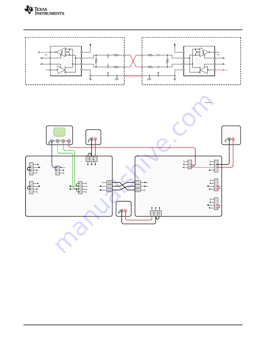
Figure 9. Wire-fault Simulation Using two EVMs
illustrates the EVM configurations and the measurement set-up. The right evaluation module
(EVM2) is configured as the driver. Both, driver and receiver enable inputs, DE and RE, receive high
potential through the wire-bridges to VCC at JMP3 and JMP2. Note that EVM2 is turned by 180°.
EVM1 on the left is configured as the receiver. Here, the driver and receiver enable inputs receive low
potential through the wire-bridges to GND at JMP3 and JMP2.
Figure 10. EVM Configurations: Left as Receiver EVM, Right as Transmitter EVM
The input data signal entering EVM2 at JMP4 is measured on scope channel 1, probing the signal at
the D-input pin of JMP14. The cross-wiring of the bus wires occurs at the EVM interlink, between the
two TB2 terminal blocks. To proof wire-fault robustness, the differential receiver input and the
single-ended receiver output signals are measured after the cross-wiring. Channels 2 and 3 measure
the bus voltages, V
A
and V
B
, at pin 2 and pin 3 of JMP6, while the receiver output is taken from pin 1 at
JMP11. Note that both 5 V power supplies, PSU1 and PSU2 have their ground terminals connected to
the ground and Earth terminals of their respective EVMs.
The scope pictures for the individual examples are shown in
,
, and
.
and
show the top and bottom view of the SN65HVD96 EVM.
7
SLLU128A – June 2010 – Revised August 2010
Sympol™ Transceiver
Copyright © 2010, Texas Instruments Incorporated


