background image

SN74LVC2G241 

(One driver)

Physical Push 

Bu tton

Microprocessor

V

CC

SN74LVC2G241

SCES210O – APRIL 1999 – REVISED DECEMBER 2015

www.ti.com

9 Application and Implementation

NOTE

Information in the following applications sections is not part of the TI component
specification, and TI does not warrant its accuracy or completeness. TI’s customers are
responsible for determining suitability of components for their purposes. Customers should
validate and test their design implementation to confirm system functionality.

9.1 Application Information
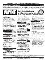
Typical Application

shows a simple application where a physical push button is connected to the

SN74LVC2G241. The push button is in a physical location far enough away from the processor that the input
signal is weak and needs to be redriven. The SN74LVC2G241 acts as a redriver, providing a strong input signal
to the processor with as little as 1 ns of propagation delay.

9.2 Typical Application

Figure 4. SN74LVC2G241 Application

9.2.1 Design Requirements

This device uses CMOS technology and has balanced output drive. Take care to avoid bus contention because it
can drive currents that would exceed maximum limits. The high drive also creates fast edges into light loads, so
routing and load conditions must be considered to prevent ringing.

9.2.2 Detailed Design Procedure

1. Recommended Input Conditions

Rise time and fall time specs. See (

Δ

t/

Δ

V) in

Recommended Operating Conditions

.

Specified high and low levels. See (V

IH

and V

IL

) in

Recommended Operating Conditions

.

Inputs are overvoltage tolerant allowing them to go as high as (V

I

max) in

Recommended Operating

Conditions

at any valid V

CC

.

2. Recommend Output Conditions

Load currents must not exceed (I

O

max) per output and must not exceed (Continuous current through V

CC

or GND) total current for the part. These limits are located in

Absolute Maximum Ratings

.

Outputs must not be pulled above V

CC

during normal operation or 5.5 V in high-z state.

10

Submit Documentation Feedback

Copyright © 1999–2015, Texas Instruments Incorporated

Product Folder Links:

SN74LVC2G241

Summary of Contents for SN74LVC2G241

Page 1: ...anslate To ensure the high impedance state during power up Inputs From a Max of 5 5 V Down or power down OE should be tied to VCC through a to the VCC Level pullup resistor and OE should be tied to GN...

Page 2: ...cs 7 12 4 Electrostatic Discharge Caution 12 6 9 Typical Characteristic 7 12 5 Glossary 12 7 Parameter Measurement Information 8 13 Mechanical Packaging and Orderable 8 Detailed Description 9 Informat...

Page 3: ...VSSOP Top View Top View YZP Package 8 Pin DSBGA Bottom View Pin Functions 1 2 PIN I O DESCRIPTION NAME NO 1A 2 I Input 1OE 1 I Output enable Active low 1Y 6 O Output 2A 5 I Input 2Y 3 O Output 2OE 7...

Page 4: ...3 The value of VCC is provided in the Recommended Operating Conditions table 6 2 ESD Ratings VALUE UNIT Human body model HBM per ANSI ESDA JEDEC JS 001 all pins 1 2000 Electrostatic V ESD V Charged d...

Page 5: ...mmended operating free air temperature range TA 40 C to 125 C unless otherwise noted PARAMETER TEST CONDITIONS VCC TA MIN TYP 1 MAX UNIT IOH 100 A 1 65 V to 5 5 V VCC 0 1 IOH 4 mA 1 65 V 1 2 IOH 8 mA...

Page 6: ...2 5 V 0 2 V 1 5 2 tdis OE Y ns VCC 3 3 V 0 3 V 1 4 2 VCC 5 V 0 5 V 1 3 3 6 7 Switching Characteristics TA 40 C to 125 C over recommended operating free air temperature range unless otherwise noted se...

Page 7: ...T CONDITIONS VCC TYP UNIT VCC 1 8 V 19 VCC 2 5 V 19 Outputs enabled pF VCC 3 3 V 20 Power dissipation VCC 5 V 22 Cpd capacitance f 10 MHz VCC 1 8 V 2 per buffer driver VCC 2 5 V 2 Outputs disabled pF...

Page 8: ...ons such that the output is low except when disabled by the output control Waveform 2 is for an output with internal conditions such that the output is high except when disabled by the output control...

Page 9: ...Figure 3 Logic Diagram Positive Logic 8 3 Feature Description To ensure the high impedance state during power up or power down OE should be tied to VCC through a pullup resistor and OE should be tied...

Page 10: ...plication Figure 4 SN74LVC2G241 Application 9 2 1 Design Requirements This device uses CMOS technology and has balanced output drive Take care to avoid bus contention because it can drive currents tha...

Page 11: ...bypass capacitor should be installed as close to the power pin as possible for best results 11 Layout 11 1 Layout Guidelines When using multiple bit logic devices inputs must not ever float In many c...

Page 12: ...ign support tools and contact information for technical support 12 3 Trademarks NanoFree E2E are trademarks of Texas Instruments All other trademarks are the property of their respective owners 12 4 E...

Page 13: ...ct NRND Not recommended for new designs Device is in production to support existing customers but TI does not recommend using this part in a new design PREVIEW Device has been announced but is not in...

Page 14: ...th Important Information and Disclaimer The information provided on this page represents TI s knowledge and belief as of the date that it is provided TI bases its knowledge and belief on information p...

Page 15: ...n1 Quadrant 74LVC2G241DCUTG4 VSSOP DCU 8 250 180 0 8 4 2 25 3 35 1 05 4 0 8 0 Q3 SN74LVC2G241DCTR SM8 DCT 8 3000 180 0 13 0 3 35 4 5 1 55 4 0 12 0 Q3 SN74LVC2G241DCUR VSSOP DCU 8 3000 180 0 8 4 2 25 3...

Page 16: ...mm Height mm 74LVC2G241DCUTG4 VSSOP DCU 8 250 202 0 201 0 28 0 SN74LVC2G241DCTR SM8 DCT 8 3000 182 0 182 0 20 0 SN74LVC2G241DCUR VSSOP DCU 8 3000 202 0 201 0 28 0 SN74LVC2G241YZPR DSBGA YZP 8 3000 21...

Page 17: ...0 8 0 15 NOM Gage Plane 4188781 C 09 02 4 25 5 0 30 0 15 2 90 3 75 2 70 8 4 3 15 2 75 1 0 10 0 00 1 30 MAX Seating Plane 0 10 M 0 13 0 65 PIN 1 INDEX AREA NOTES A All linear dimensions are in millime...

Page 18: ......

Page 19: ...GRID ARRAY NOTES 1 All linear dimensions are in millimeters Any dimensions in parenthesis are for reference only Dimensioning and tolerancing per ASME Y14 5M 2 This drawing is subject to change withou...

Page 20: ...continued 3 Final dimensions may vary due to manufacturing tolerance considerations and also routing constraints For more information see Texas Instruments literature number SNVA009 www ti com lit sn...

Page 21: ...P 4223082 A 07 2016 DSBGA 0 5 mm max height YZP0008 DIE SIZE BALL GRID ARRAY NOTES continued 4 Laser cutting apertures with trapezoidal walls and rounded corners may offer better paste release SYMM SY...

Page 22: ......

Page 23: ......

Page 24: ...TI Resource NO OTHER LICENSE EXPRESS OR IMPLIED BY ESTOPPEL OR OTHERWISE TO ANY OTHER TI INTELLECTUAL PROPERTY RIGHT AND NO LICENSE TO ANY TECHNOLOGY OR INTELLECTUAL PROPERTY RIGHT OF TI OR ANY THIRD...

Reviews: