


TI Information – Selective Disclosure SLOU
PurePath™ Smart Amp User Manual (TAS5766M/68M)
31
5.3
Power Supply Current at Higher Frequencies
Power supply current is limited by its inductance at higher frequencies, which is due to a
combination of the power supply itself, passives and PCB layout. The PWM output stage of a
Class-D amplifier switches at a high frequency (>100 kHz) which may cause the power supply
voltage to drop if not decoupled properly affecting the amplifier and other circuits as well.
An LC filter at the output of a Class-D amplifier helps reduce high frequency switching current
through the load and from the power supply while increasing efficiency. Some applications
restrained by cost/space may use ferrite beads instead of the traditional LC filter, taking into
advantage the series inductance of the loudspeaker. The design of Class-D filters is discussed
in [
]. An LC filter is a second order filter, damped by the load impedance. The filter values are
usually calculated based on the DC resistance of the loudspeaker. However, the filter may
become underdamped due to the corner frequency of the filter and the inductance of the
loudspeaker. An underdamped response will manifest as a dip in the impedance which may
cause currents higher than the ones calculated for the rated loudspeaker impedance. For this
reason, it is recommended to implement a snubber circuit in parallel to the filter capacitors. The
device evaluation module (EVM) and datasheet are the best reference for these filters.
The PWM signal must have good integrity in order to provide a good fidelity output signal. As
mentioned previously, the power supply and PCB layout may not be capable of delivering the
initial switching current required by the PWM signal. The worst-case scenario would involve
calculating the bulk capacitor based on peak current delivered into the load, switching frequency
and acceptable ripple. However, the ripple voltage may be dominated by the capacitor series
resistance (ESR) in most cases [
]. Larger capacitor sizes may have a larger series inductance
(ESL), so it is recommended to have smaller decoupling capacitor in parallel to compensate. As
with the output filters, the device EVM and datasheet are the best reference for decoupling
capacitor selection.
5.4
Post-processing Considerations
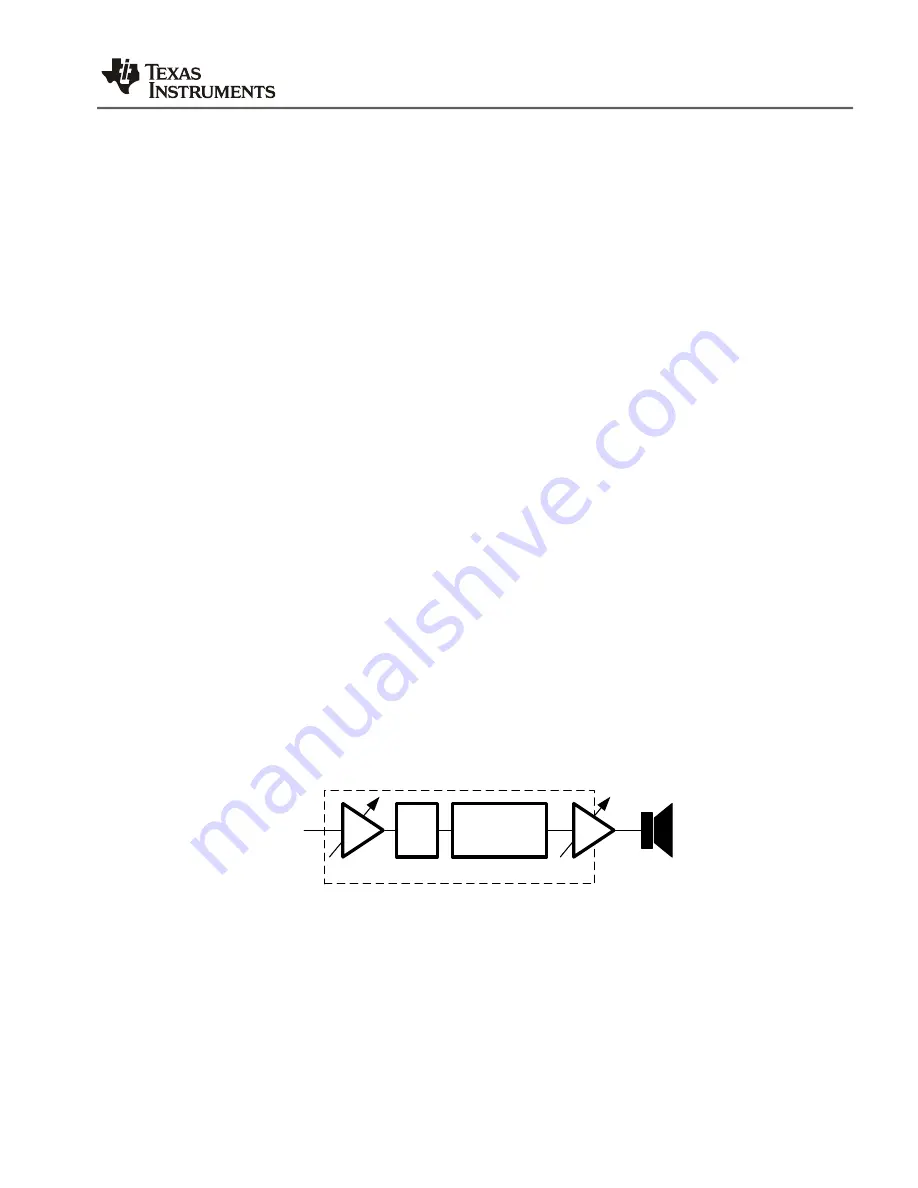
The Smart Amp signal chain is comprised of pre-processing, the Smart Amp algorithm and
output gain controls (G
O
). Pre-processing includes input volume controls (G
I
) and custom
equalization filters. Any changes that occur after the Smart Amp algorithm (post-processing) will
affect how Smart Amp understands a speaker and acts on it.
Smart Amp
Processing
G
O
in
EQ
G
I
Digital Processing
Figure 12. Smart Amp Signal Chain
Smart Amp devices have register-based output gain controls and may also have hardware pin
gain control for the output amplifiers. It is recommended to set the gain level such that the full-
scale voltage output (V
pk,FS
) is close to the desired maximum power supply current per channel.
In most circumstances, the gain should be set such that the peak output voltage is close to the
supply voltage (V
dd,sa
), but if the supply voltage is much higher, then the current can be
controlled by lowering the post-processing gain.


